Root cause analysis (RCA) of shrinking device geometries and process integration is becoming increasingly challenging. The contaminants limiting yield are often monolayer organic residues and sub-20 nm particles, which are below the spatial resolution and outside the chemical specificity of typical analytical techniques.
Contaminants come from process-induced, material-related, environmental, or handling sources, and they may pass through multiple process steps before producing noticeable effects.
RCA seeks to trace these effects, which can manifest as parametric drift, reliability issues, or bonding faults in advanced packaging, back to their source.
In current RCA workflows, inspection technologies like KLA Surfscan use optical methods to assess the distribution of defects, allowing engineers to draw conclusions about defect origin. For example, spatial clustering can indicate equipment contamination, whereas random distributions can indicate airborne exposure.
While this data is useful, chemical identification of defects offers failure analysis teams critical causality information. As device geometries shrink and heterogeneous integration multiplies material interfaces, RCA must resolve organic flaws smaller than 20 nm, which are beyond the capabilities of currently available analytical techniques.
PiFM for Semiconductor RCA
Photo-induced Force Microscopy (PiFM) is uniquely suited for use in semiconductor RCA because it is the only analytical technique that combines sub-5 nm spatial resolution, molecular identification, monolayer sensitivity, and nondestructive measurement (Table 1).
This exact combination of capabilities is lacking in widely used techniques such as SEM/EDS and ToF-SIMS on sub-20 nm and organic defects.
PiFM is a non-contact atomic force microscopy and infrared spectroscopy (AFM-IR) method for identifying chemical species by directly measuring the photo-induced force between the AFM probe and the sample.
It generates spectra that are remarkably similar to those of equivalent bulk FTIR spectra and can be searched directly against commercial or user-created IR libraries for identification.
PiFM, like FTIR, identifies organic and inorganic materials. However, because PiFM detects the PiF through the mechanical response of the cantilever, the technique can also provide useful information on "IR inactive" materials such as pure metals and 2D materials.
The AFM probe's near-field amplification of the IR laser improves the spatial resolution of IR spectroscopy to better than 5 nm. PiFM can spatially map nanometer-scale patterns of individual chemical components by imaging at multiple IR wavelengths corresponding to different chemical species' absorption maxima.1
Especially when performing RCA, PiFM delivers three capabilities that other analytical approaches cannot:
- Molecular identification at the defect length scale: With sub-5 nm lateral resolution and monolayer sensitivity, a defect with a thickness of approximately 1 nm can be resolved and chemically characterized in a single test.
- Non-destructive, ambient operation: This eliminates the requirement for vacuum or sample preparation, such as sputtering or electron-beam exposure.
- Identification of organics: PiFM can easily identify organic defects, such as photoresist residues, BARC residues, adhesion promoters, and bonding inhibitors, due to their strong IR absorption. These are the materials most likely to cause current yield failures, but they are invisible or ambiguous in EDS.
Where SEM/EDS, ToF-SIMS, and Other Analytical Techniques Fall Short
When a defect is primarily organic, a monolayer residue, or less than 20 nm in size, SEM/EDS, ToF-SIMS, and TEM/STEM-EDS all fail a different phase of the RCA workflow.
SEM/EDS provides high-resolution morphological imaging at the nanoscale, but because EDS captures elemental rather than molecular information, the material cannot be identified.
SEM-based EDS spatial resolution is also limited by the electron-beam interaction volume of around 0.5 µm, more than two orders of magnitude bigger than the defects currently dictating yield.
Finally, e-beam irradiation can erase minor flaws and frequently deposits hydrocarbons on the sample, contaminating the signal that an analyst is attempting to decipher.
ToF-SIMS gives molecular information and high trace sensitivity, but its lateral resolution of 0.2–10 µm is insufficient to detect defects smaller than 20 nm. ToF-SIMS is also damaging due to ion sputtering and is susceptible to matrix effects, which complicate the identification of organic compounds and thin films.
TEM/STEM-EDS provides atomic-scale imaging but necessitates destructive FIB cross-sectioning and yields elemental rather than molecular data. XPS, TXRF, and Auger are useful in certain situations, but they are either too large in analysis spot size (XPS, TXRF) or too limited in chemistry (Auger) for nanoscale organic RCA (Table 1).
Table 1. Comparison of IR PiFM against standard analytical techniques used in semiconductor RCA. IR PiFM is the only technique that combines sub-5 nm lateral resolution with molecular identification and monolayer depth sensitivity. Source: Molecular Vista
| |
IR PiFM |
TOF-SIMS |
XPS |
SEM/EDS |
TEM |
TXRF |
Auger |
| Species Detected |
Molecular |
Molecular |
Molecular |
Elemental |
Elemental |
Elemental |
Elemental |
| Lateral Resolution |
<5 nm
∼20 nm* |
>0.2 μm |
10 μm - 2 mm |
1 nm imaging
0.5 μm EDS |
0.2 nm imaging
1∼20 nm EDS |
∼1 mm |
∼10 nm |
| Depth Probed |
<20 nm
∼500 nm* |
1 nm |
10 nm |
1 μm |
∼100 nm |
10 nm |
10 nm |
* Bulk mode
How PiFM Shortens the RCA Workflow
PiFM on the Vista 300 integrates with standard fab inspection workflows by accepting KLARF defect maps directly from inline inspection tools such as KLA Surfscan; auto-deskewing to wafer fiducials (typically a few larger defects); and sequentially visiting each defect of interest (DOI) to acquire topography and PiF-IR spectra (Figure 1).
Typical throughput on the Vista 300 is one to two minutes per defect, depending on the accuracy of the inspection tool's coordinates, therefore enabling chemical-ID surveys of 30 to 50 flaws in about one hour.
PiFM is not intended to be a complete replacement for SEM/EDS, but rather to work alongside these instruments. Current SEM/EDS tools have a throughput of approximately one order of magnitude higher than Vista 300 ANDR. As a result, when multiple larger inorganic/metallic flaws must be classified by shape and elemental composition, SEM/EDS can remain the workhorse.
The defects that SEM/EDS cannot accurately characterize, such as sub-20 nm particles, organics, and monolayer residues, should be sent to the Vista 300 ANDR for PiFM analysis. This eliminates the need for speculative follow-up using ToF-SIMS or destructive TEM.
Following characterization, the physical findings must be linked to the contaminated source. Using PiFM, nanodefects can be discovered quickly, enabling a faster transition from characterization to correlation investigations and shortening the RCA loop for defect classes that frequently limit yield at advanced nodes.
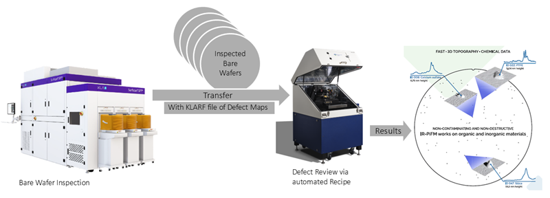
Figure 1. KLARF-driven automated nano defect review (ANDR) workflow. Defect coordinates from an inline inspection tool are imported to the Vista 300, which navigates to each DOI and returns both topographic and molecular chemical identification at nanometer resolution. Image Credit: Molecular Vista
RCA with PiFM Case Studies
PiFM is commonly used to handle RCA issues. The three examples below are based on data previously published in a Molecular Vista application note.2 These examples demonstrate how PiFM replaces inference with direct identification.
Case 1: 3 nm Silica Particle on Silicon
A 3 nm-tall particle on a silicon surface produced a PiF-IR spectrum with a blue peak at 1085 cm−1 (see Figure 2). A library search of the Wiley KnowItAll database yielded a straight match to silica (top set of spectra).3
No inference was necessary. A single PiFM measurement transformed an unidentified particle of interest on an inspection map into a designated contaminant that could be linked to a specific tool, wet-chemistry phase, or polishing slurry.
SEM/EDS would not have been able to analyze a particle of this size; even if it had, it would have recorded Si and O without distinguishing between the silicon substrate and its natural oxide.
The red spectrum acquired on the substrate next to the defect shows peaks at ∼1100, 1460, and 2940 cm−1, which are associated with native silicon oxide and a hydrocarbon contamination layer on the substrate surface, demonstrating the monolayer sensitivity of IR PiFM.
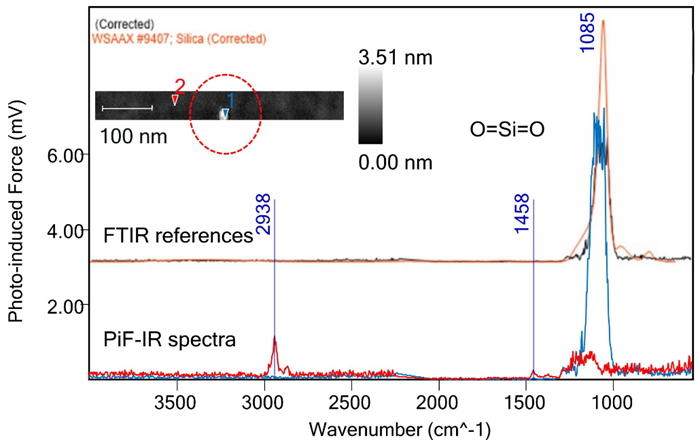
Figure 2. PiF-IR spectrum from a 3 nm particle on a silicon surface, identified as silica by searching the Wiley KnowItAll IR library. Inset: AFM topography of the particle (red dashed circle). Image Credit: Molecular Vista
Case 2: ∼1 nm PFPE Monolayer on a “Clean” Wafer
Five PiF-IR spectra from different positions of a wafer retrieved from a storage container were repeatable and showed a dominating peak at ∼1250 cm−1, in addition to the silicon oxide signal at 1130 cm−1.
Averaging the spectra and scanning the IR library revealed that the contaminant layer was perfluoropolyether (PFPE), a contact-transfer contamination from the storage container (Figure 3a), which could have been derived from PFA (Perfluoroalkoxy alkanes).
Following plasma cleaning, the same wafer exhibited a distinct fingerprint, predominantly hydrocarbon (Figure 3b), demonstrating both the efficiency of removing the PFPE monolayer and the formation of hydrocarbon pollutants during the cleaning procedure.
For an RCA team, this is a critical example: a monolayer contaminant that is invisible to optical inspection, indistinguishable in EDS, and beyond the lateral reach of ToF-SIMS was detected and, importantly, identified. This allowed the wafer carrier to be identified as the potential root cause and enabled quick corrective action at a specific point rather than a generic "improve handling" recommendation.
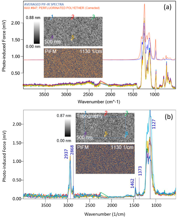
Figure 3. (a) Five PiF-IR spectra of a supposedly blank Si wafer, showing fluorocarbon (PFPE) contamination from a storage container. (b) Five more spectra on the same wafer after plasma cleaning. Image Credit: Molecular Vista
Case 3: Cu–BTA Residue After Chemical Mechanical Planarization (CMP) in Hybrid Bonding
Hybrid bonding for improved packaging requires copper surfaces free of organic inhibitors and carbides, which limit the development of real Cu-Cu interfacial grains. Benzotriazole (BTA), an inhibitor used to preserve recessed copper lines, is known to leave a thin Cu(II)-BTA polymer on the copper’s surface that is difficult to remove.4
Figure 4 shows four averaged PiF-IR spectra of Cu: (a) as electroplated, (b) after BTA treatment, (c) after a CMP process, and (d) after Ar-ion cleaning.
Figures 4b (before CMP) and 5c (after CMP) show the Cu-BTA signature, which includes peaks at ∼795 and ∼755 cm−1 from the benzene ring's C-H stretches. This suggests that BTA remains on the Cu surface throughout the CMP process.
This provided direct, process-specific proof of a residue that would otherwise be inferred from XPS elemental data or speculative chemistry from ToF-SIMS.4 After Ar-ion cleaning, the BTA signature is essentially removed (Figure 4d), indicating that the corrective treatment has closed the RCA loop on this contamination source.
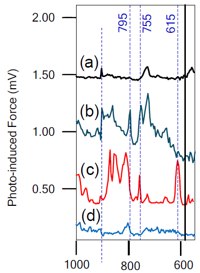
Figure 4. Averaged PiF-IR spectra for copper surfaces at successive process steps: (a) as electroplated; (b) after BTA treatment; (c) after CMP; (d) after Ar-ion cleaning following CMP. Image Credit: Molecular Vista
When to Use PiFM for RCA
PiFM on Vista 300 is the appropriate RCA tool for wafer defects that are small (less than 20 nm), predominantly organic, a residue, or otherwise "invisible" to SEM/EDS or ToF-SIMS.
Even for inorganic defects smaller than 20 nm, the low-energy X-ray peaks of many oxides may overlap, making it impossible to confidently identify the defect. Normally, other higher energy X-ray peaks would aid in identification but with minor flaws, as greater acceleration voltage could destroy the particles.
PiFM works alongside existing inline ADR workflows, closing the RCA loop in hours rather than days or weeks, thanks to its ability to give molecular rather than elemental identification. Split-lot experiments and controlled process adjustments are then used to test a specific hypothesis rather than looking for one that is reasonable.
Key Takeaways
- PiFM bridges the gap between SEM/EDX and ToF-SIMS for root cause analysis (RCA). Specifically, the combination of molecule identification at sub-5 nm resolution and monolayer sensitivity.
- PiFM is a non-destructive and effective method for detecting impurities on both organic and inorganic materials. It does not require any additional sample preparation, unlike SEM/EDX or ToF-SIMS, making it an excellent choice to find contaminants without modifying the surface.
- PiFM shortens the RCA loop by instantly identifying residues and flaws, enabling engineers to do correlation studies.
- The Vista 300 ANDR analyzes KLARF defect maps in approximately one minute, allowing for full-wafer chemical-ID surveys in around one hour (50 defects).
References and Further Reading
- Nowak, D., et al. (2016). Nanoscale chemical imaging by photoinduced force microscopy. Science Advances, 2(3). DOI: 10.1126/sciadv.1501571. https://www.science.org/doi/10.1126/sciadv.1501571.
- Molecular Vista (2016). Analyzing sub-20 nm defects and ultrathin (∼1 nm thick) residues in semiconductor processes | Molecular Vista. Molecular Vista. Available at: https://molecularvista.com/applications/analyzing-sub-100-nm-particulate-defects-and-ultrathin-1-nm-thick-residues-in-semiconductor-processes/.
- Wiley Science Solutions. (2025). KnowItAll IR Spectral Database Collection - Wiley Science Solutions. Available at: https://sciencesolutions.wiley.com/solutions/technique/ir/knowitall-ir-collection/.
- Gao, B., et al. (2019). A study of FTIR and XPS analysis of alkaline-based cleaning agent for removing Cu-BTA residue on Cu wafer. Surface and Interface Analysis, 51(5), pp.566–575. DOI: 10.1002/sia.6623. https://analyticalsciencejournals.onlinelibrary.wiley.com/doi/abs/10.1002/sia.6623.

This information has been sourced, reviewed, and adapted from materials provided by Molecular Vista.
For more information on this source, please visit Molecular Vista.