Photo-induced force microscopy (PiFM) is a sophisticated nanoscale characterization approach that combines the elevated spatial resolution of atomic force microscopy (AFM) with infrared (IR) spectroscopy’s chemical specificity.
A tunable IR laser is angled at the probe’s tip, generating a tip-enhanced field that interacts with the sample and leaves a photo-induced force signal (Figure 1).
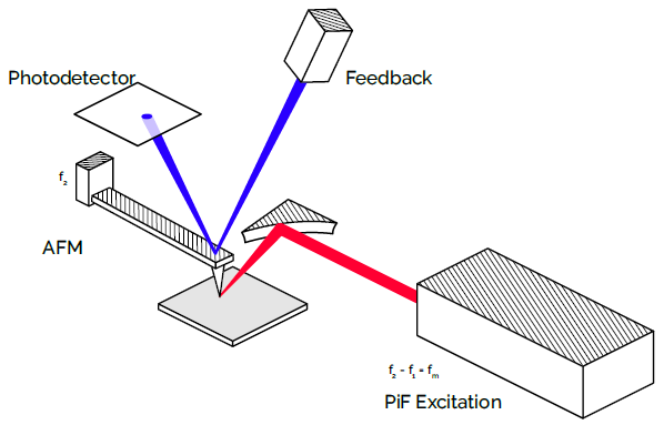
Figure 1. The PiFM instrument is built upon a non-contact AFM operating in the attractive regime. By positioning an excitation laser to the AFM tip, both the photo-induced signal from the chemical nature of the sample and topography of the sample can be recorded simultaneously by the photodetector. Image Credit: Molecular Vista
Sweeping the IR laser over appropriate wavenumbers generates PiF-IR spectra that directly correlate with FTIR spectral signatures, making it possible to achieve chemical identification that is confident and precise at the nanoscale.
Employing the AFM cantilever in its second mechanical resonance and in noncontact mode facilitates high-resolution topographical imaging without needing to physically contact the surface, minimizing the risk of tip wear and sample contamination alike.
As the AFM probe and IR laser are maintained at complementary frequencies, PiFM is able to isolate chemical and topographical signals, enabling physical and chemical mapping simultaneously with < 5 nm spatial resolution, as demonstrated in Figure 2. This ability enables PiFM to examine defects in monolayers, ALD films, polymer residues, process contaminants, and sub-100 nm semiconductors.
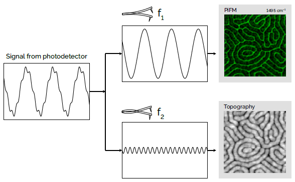
Figure 2. The photodetector signal is separated into chemical (top) and topographical (bottom) channels by modulating the AFM cantilever at its second eigenmode (f2) and the IR laser at the difference frequency (f2 - f1). This modulation creates a detectable sideband frequency at the sample's first eigenmode (f1), which the cantilever resonates with, enabling simultaneous recording of PiFM spectroscopy and AFM topography. Image Credit: Molecular Vista
ADR: Current Analytical Approach
Identifying defects on wafers is crucial, as even small defects can critically affect chip performance and yield downstream. The task of reviewing defects has previously depended on automated SEM/e-beam and EDX/EDS tools, which enable both high-resolution 2D imaging and elemental composition.
However, they cannot provide molecular data, something which is crucial for characterizing organics. Although it provides good structural detail, electron beams consistently harm samples and defects alike, making it painstaking to assess volatile, low-melting organic, and other fragile materials.
ADR: PiFM Advances the Field
PiFM overrides significant constraints inherent to conventional ADR technologies that find difficulty in assessing defects that are increasingly small and complex, like those that emerge from organic residues, composite contamination, and monolayer films that SEM, EDX, and TEM are typically unable to consistently identify or differentiate, to facilitate cutting-edge characterization of nanoscale defects.
Crucially, existing ADR workflows do not have non-destructive chemical identification tools that can resolve such features, particularly when the defect lacks visibility or is difficult to discern under electron-based review.
Organic and inorganic nanosized defects alike are receptive to physical damage, being altered by chemicals, and mass loss following SEM/EDX analysis, something which makes comprehensive examination of ultra-small defects challenging in the present workflow.1
It is possible that PiFM can take on this challenge directly as it can chemically and topographically distinguish defects that are as small as 5 nm and generate correlated maps that identify true defect materials from background texture and cleaning artifacts alike, even on bare silicon and complex multilayer coatings.
On a wafer recently examined by Molecular Vista, the company was able to distinguish e-beam damage from former analysis at marked defect coordinates from SEM/EDS analysis and unaffected defects, which they were also able to characterize without generating further damage (Figure 3).
Furthermore, Molecular Vista’s Vista 300 tool has the ability to directly navigate to KLARF (KLA Tencor Advanced Results File) defect coordinates on 300 mm wafers, which significantly heightens ease of defect location, a significant time bottleneck in the defect review process, and greatly increases productivity.
Molecular Vista has been able to significantly increase its defect identification output, as demonstrated in Figure 4. Lastly, as PiFM is non-contact, the wafers and defects stay intact for re-inspection and analysis downstream, removing unnecessary re-preparation of samples.
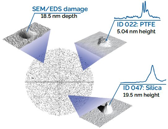
Figure 3. A KLARF map of a 300 mm wafer shows successful, non-destructive PiFM analysis of two defects (ID 022 and ID 047) identified as PTFE and silica, respectively. This contrasts with a destructive SEM/EDS measurement that created an 18.5 nm crater. Image Credit: Molecular Vista
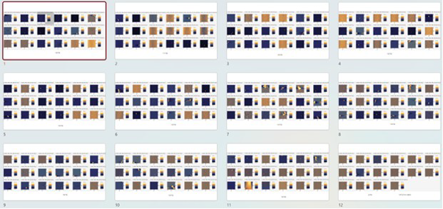
Figure 4. The result of hundreds of defects reviewed with PiFM in auto recipe mode from one overnight run, acquiring both topography and PiFM spectral data on and off defects (substrate). Image Credit: Molecular Vista
Conclusion
As semiconductor manufacturing continues to advance and devices become smaller, demands for defect analysis and review capabilities increase.
By delivering definitive chemical identification of organic, inorganic, and complex mixed-material defects in a completely non-destructive way, PiFM maintains wafer and device integrity for continued examination while producing sub-5 nm chemical imaging of defects that stay invisible to traditional review tools.
This mix of nanoscale resolution, direct mapping from the inspection tool’s defect coordinates, and support for 300 mm workflows delivers actionable insights that accelerate yield learning, identify root causes, and facilitate confident, data-driven process enhancements.
Such PiFM abilities make it a robust tool for automating defect review in advanced semiconductor manufacturing.
References and Further Reading
- Schmied, M. and Poelt, P. (2002). Particle Analysis by SEM/EDXS and Specimen Damage. Microchimica Acta, 139(1-4), pp.171–177. DOI: 10.1007/s006040200057. https://link.springer.com/article/10.1007/s006040200057.

This information has been sourced, reviewed and adapted from materials provided by Molecular Vista.
For more information on this source, please visit Molecular Vista.