Save time and boost confidence in wafer quality evaluation via automated full-wafer Raman screening on the RMS1000 with WaferMAP.
- In the Ramacle Python IDE, RamanQA guarantees high sensitivity and dependable wafer quality assurance by combining peak parameter and multivariate pass/fail thresholding of the spectral dataset
- Results are automatically organized into detailed, audit-ready reports that feature maps, tables, and histograms, allowing engineers to rapidly identify problem regions and make informed quality decisions
In semiconductor fabrication, fast and dependable wafer quality screening is essential for safeguarding yield and speeding up production. Conventional inspection techniques, including optical microscopy and electrical testing, provide limited visibility into subsurface structures and material inconsistencies, which may result in device performance variation or downstream failures.
Confocal Raman microscopy provides a non-destructive, highly sensitive method for examining material characteristics across a full wafer. Fitted with WaferMAP® and integrated with the RamanQA Python module, the RMS1000 Confocal Multimodal Microscope (Figure 1) transforms this ability into a completely automated quality assurance process.
RamanQA extracts essential spectral parameters, applies tolerance thresholds, and uses multivariate evaluation to produce objective pass/fail decisions.
This article illustrates how RamanQA can quickly evaluate semiconductor wafer quality, automatically generate pass/fail maps, and deliver practical insights for engineers and scientists. By integrating high-throughput data collection with robust statistical evaluation, RamanQA supports faster, more reliable wafer screening while simplifying both routine quality control and comprehensive defect diagnostics.
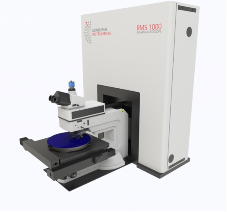
Figure 1. An Edinburgh Instruments RMS1000 Confocal Multimodal Microscope with WaferMAP functionality. Image Credit: Edinburgh Instruments
RamanQA Step-by-Step Methodology
The RamanQA workflow uses automated spectral feature extraction and statistical tolerance evaluation across extensive wafer datasets. The process is outlined below:
1. Data Collection in WaferMAP
In WaferMAP, Raman spectra are gathered across a wafer to produce an image dataset containing hundreds or thousands of spectra. Each spectrum represents the condition of a small area of the wafer surface and contains data regarding localized strain, defects, material variations, or surface imperfections.
2. Raman Peak Feature Extraction
For each spectrum, the primary wafer Raman mode (e.g., 520 cm-1 for Si, 567 cm-1 for GaN, 1581 cm-1 for graphene) is identified, and the peak intensity, position, and full width half maximum (FWHM) are extracted (Table 1). These parameters serve as the primary physical wafer quality metrics.
Table 1. Peak parameters extracted in RamanQA and the likely physical causes of variance in them across a semiconductor wafer. Source: Edinburgh Instruments
| Peak Parameter |
Likely Cause of Variance in Parameter |
| Peak Intensity |
Crystallinity, doping, surface contaminants |
| Peak Position (cm-1) |
Strain, doping, crystallinity |
| FWHM (cm-1) |
Disorder, defects, strain |
Across all acquisition points, median values are calculated for each extracted spectral parameter. These median values establish the wafer’s expected “normal” Raman response. Alternatively, the expected response can be defined using historical data when the same wafer type is repeatedly analyzed over an extended period.
3. Multivariate Spectral Consistency Evaluation
RamanQA also offers optional multivariate evaluation to identify subtle spectral deviations that are not detected through semiconductor peak metrics alone. For instance, deviations from a non-fluorescent contaminant with spectral features that do not overlap with the semiconductor band(s) under examination.
The two available evaluation tools are Pearson correlation and Mahalanobis distance (MD). Including both ensures robustness and sensitivity for both quantitative and qualitative spectral deviations. A technical deep dive into these techniques is available in the appendix for readers seeking additional information.
4. Tolerance Window Selection
User-defined tolerance thresholds (e.g., ±2 cm-1 for position, ±20% for peak intensity and FWHM) are applied. Each spectrum is subsequently classified according to whether all parameters fall within these acceptance windows. Tolerances are also established for Pearson correlation and MD.
For Pearson correlation, an r value of 0.95 is considered a good match to the median wafer spectrum, while spectra with an r value below 0.9 to the median likely indicate defects or contamination.
For MD, a practical threshold is 3. This serves as a robust statistical filter: any value greater than 3 signifies more than a 99% probability of abnormal wafer behavior at that point.
5. Pass Rate Determination
A wafer pass rate is determined as the percentage of spectra that fulfill all chosen requirements (tolerance thresholds and optional multivariate assessments).
6. Final Classification
The wafer is classified as pass if the pass rate surpasses the user-defined acceptance level (fully customizable); otherwise, it is classified as fail. This framework supports both high-throughput routine screening and comprehensive defect diagnostics.
7. Mapping of Pass/Fail Regions and Visualization
RamanQA automatically generates wafer-scale visual outputs, including:
- An overall pass/fail map showing which pixels satisfy all tolerance requirements
- Peak feature maps illustrating spatial fluctuations in peak position, intensity, and FWHM
- A Pearson correlation map identifying spectra with low correlation to the wafer-average spectrum
- A PCA MD map highlighting statistical outliers in multivariate spectral space
Additionally, histograms and box plots are generated for each metric to summarize wafer-wide distributions, providing quantitative insight into variability, deviations, and outlier behavior.
All results are compiled into a PDF report that combines wafer maps, plots, and tabulated metrics, delivering a comprehensive and actionable overview of wafer quality.
RamanQA Demonstration on a Real Wafer
To demonstrate the RamanQA process, a full-wafer Raman dataset was obtained from a four-inch carbon nanotube/silicon wafer using WaferMAP on the RMS1000, selected intentionally due to the high level of variability across the wafer.
A total of 17,560 spectra were gathered over the wafer surface with a step size of 650 µm. Figure 2 illustrates the Raman intensity map at the 520 cm-1 silicon phonon mode in WaferMAP, highlighting variations in the optical response.
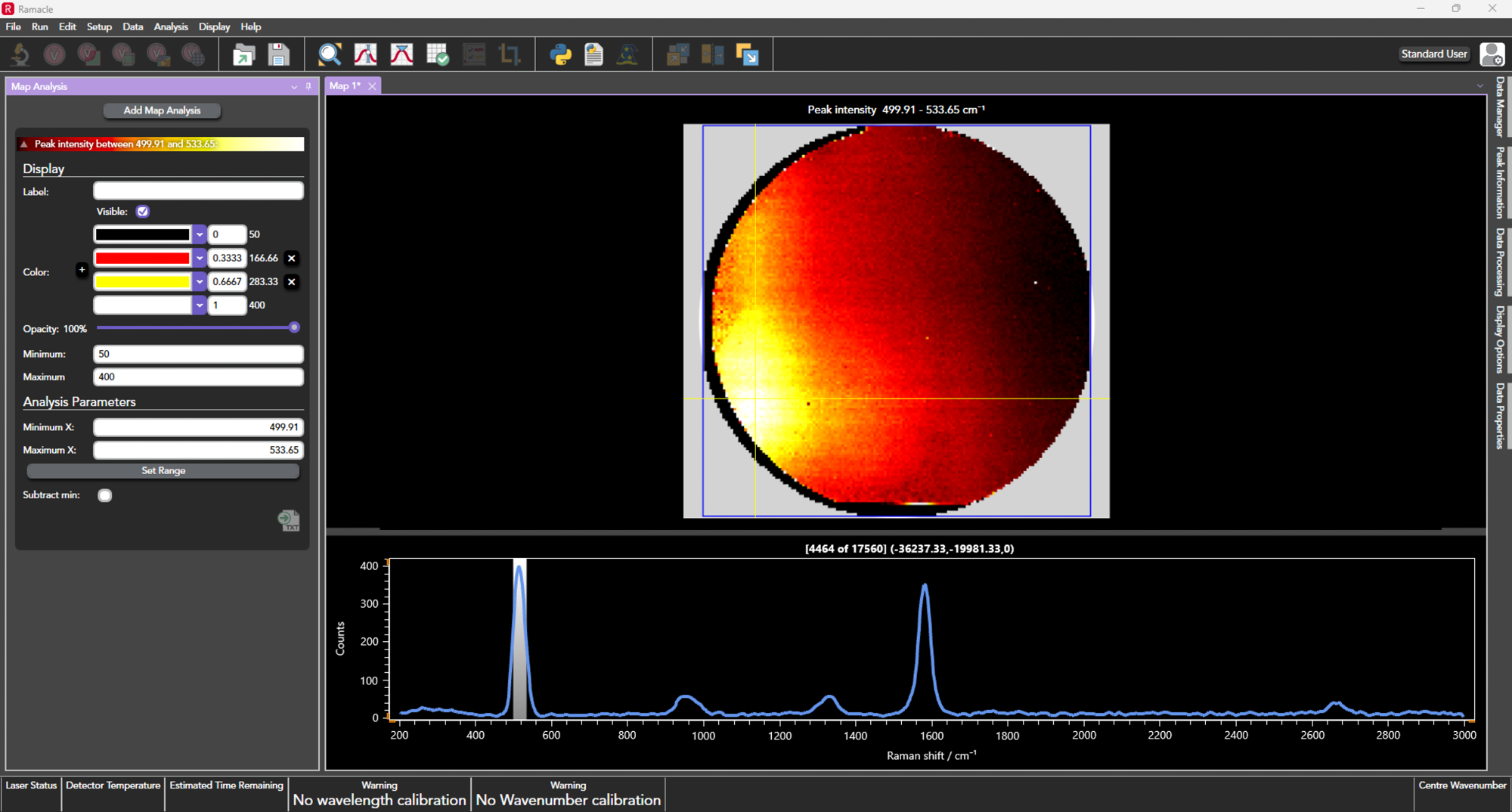
Figure 2. Raman intensity map of the 520 cm-1 phonon mode acquired from a four inch carbon nanotube/silicon wafer in WaferMAP. Image Credit: Edinburgh Instruments
The RamanQA Python IDE module was used to extract all spectra, fit the 520 cm-1 band, and calculate peak intensities, positions, and FWHMs of the band at each pixel. For the purposes of this article, the tolerance windows for the peak parameters as well as the multivariate Pearson correlation and MD functions were set as follows:
- Intensity: +/- 50% from median
- Position: +/- 2 cm-1 from median
- FWHM: +/- 20% from median
- Pearson minimum r: 0.9 against median
- Maximum MD: 3
The pass threshold was set at 90% of all spectra, requiring 90% of spectra to fall within all set tolerance windows in order to pass. A spectrum was set to fail if even a single parameter fell outside its tolerance window. The findings are displayed in Table 2. Based on the 90% threshold, the overall result was a fail.
Table 2. Results for RamanQA of the carbon/nanotube silicon wafer by tracking the silicon band. Source: Edinburgh Instruments
| Metric |
Tolerance |
% Passed |
| Silicon peak intensity |
+/-50% from median |
68.85 |
| Silicon peak position |
+/-2 cm-1 from median |
73.64 |
| Silicon peak FWHM |
+/-20% from median |
99.41 |
| Pearson correlation r |
>0.9 against median |
55.77 |
| MD |
<3 |
94.92 |
| Wafer Result |
FAIL (peak intensity, peak position, Pearson correlation) |
Figure 3 presents classification wafer maps, indicating where the wafer failed for each metric. These were output by RamanQA, as well as histograms and boxplots showing the magnitude of the variance within each matrix. These plots are automatically compiled in an in-depth PDF report.
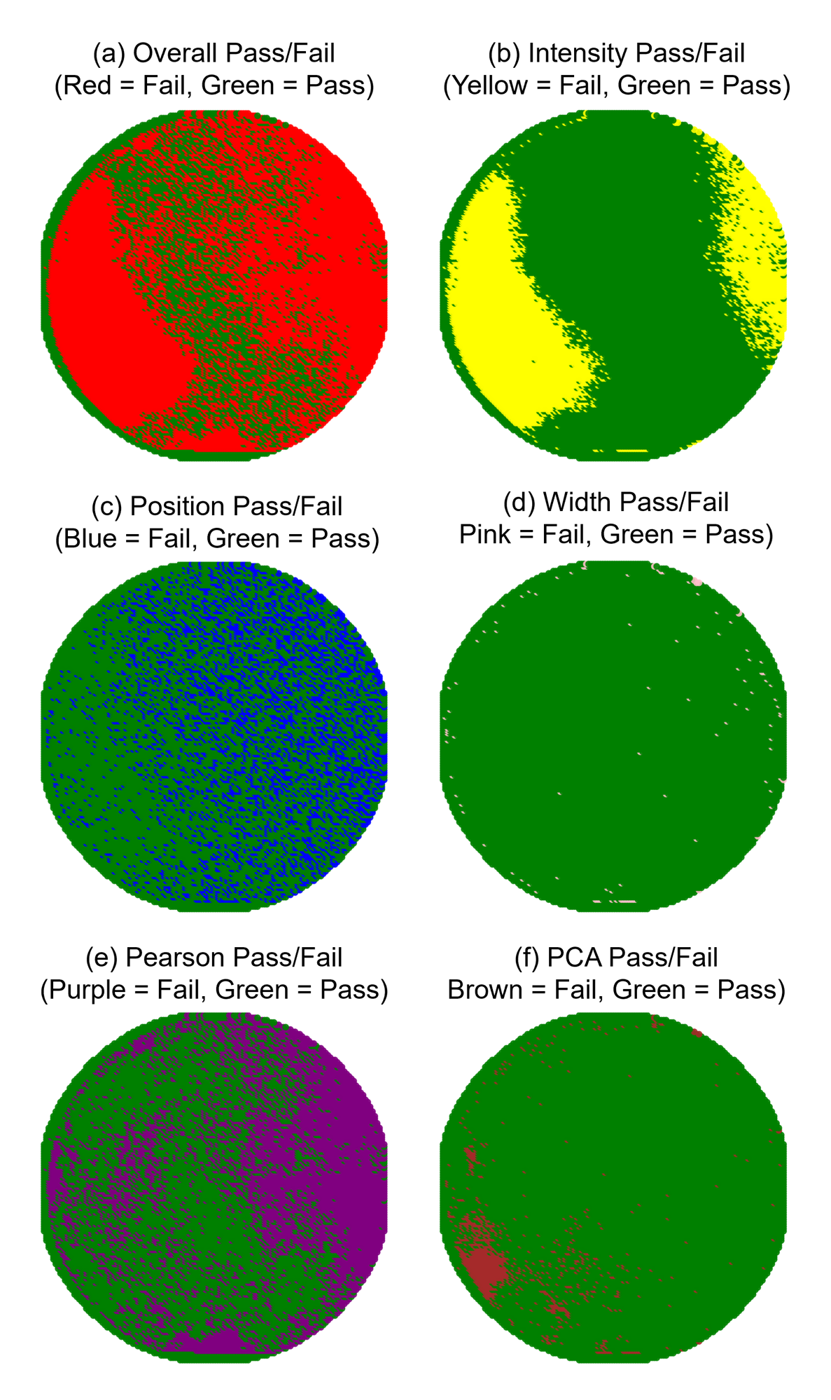
Figure 3. Wafer pass/fail analysis across multiple metrics using RamanQA. (a) Overall wafer pass/fail map (red = fail, green = pass). (b–f) Individual feature fail maps: (b) peak intensity (yellow = fail, green = pass), (c) peak position (blue = fail, green = pass), (d) FWHM/width (pink = fail, green = pass), (e) Pearson correlation (purple = fail, green = pass), and (f) Mahalanobis distance (brown = fail, green = pass). Image Credit: Edinburgh Instruments
The most probable physical cause for the widespread variation in both the silicon peak intensity and the overall spectral profile (especially the low Pearson correlation with the median) is inconsistent carbon nanotube (CNT) coverage across the wafer surface.
The nanotube layer is positioned on top of the silicon substrate. Fluctuations in CNT film thickness, density, or overall coverage would directly impact the intensity of the underlying silicon Raman peak due to scattering, absorption, or interference effects. The low pass rate for intensity confirms substantial heterogeneity across the wafer.
Similarly, inconsistent CNT coverage means that some regions may exhibit the strong silicon peak and CNT spectral characteristics, while others may show only the silicon peak or exhibit it with varying degrees of suppression. This significantly alters the overall spectral shape, resulting in a low Pearson correlation coefficient and, consequently, a low pass rate.
Conclusion
By combining the RMS1000 with WaferMAP high-throughput data acquisition and automated spectral response statistics through the Python IDE, RamanQA delivers a powerful, non-destructive, and objective framework for semiconductor wafer quality assurance.
Through the automatic extraction of crucial material and semiconductor spectral parameters (peak position, intensity, FWHM), as well as robust multivariate evaluation (Pearson correlation and MD) against user-defined tolerances, RamanQA quickly converts complicated spectral datasets into clear, actionable pass/fail decisions and spatial defect maps.
It is worth noting that RamanQA is completely customizable and can be pivoted for any semiconductor material. It is also possible to extract peak intensity ratios and the splitting of the Raman shift between two semiconductor bands, depending on the specific material being analyzed.
These capabilities allow semiconductor producers to simplify wafer inspection, quickly detect localized anomalies, and speed up both high-throughput screening and in-depth failure diagnostics.
Appendix
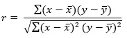
In RamanQA, the Pearson correlation function determines how closely each spectrum corresponds to the wafer-average spectral profile. It is described in Equation 1.
 |
(1) |
In this equation, x is the spectrum being evaluated, and y is the wafer-average spectrum. An r coefficient of one shows that the spectrum is in perfect agreement with the median wafer spectrum. As the spectral signature grows increasingly distorted due to a physical or chemical phenomenon on the wafer, r approaches zero.
By comparison, the Mahalanobis distance (MD) measures how far each spectrum lies from the statistical center of wafer behavior, while considering the variance and covariance of multiple spectral characteristics concurrently.
In RamanQA, principal component analysis (PCA) reduces each spectrum to several key components that capture the primary spectral data patterns. MD then determines a single distance value in this PCA space, as demonstrated in Equation 2.
 |
(2) |
In this equation, x represents the spectrum’s PCA score vector (i.e., it contains scores for each PC), µ is the average PCA score vector (the wafer ‘centroid’), and S is the covariance matrix of the PCA scores.
It should be noted that D2 represents the squared MD and that reporting D2 is more common for quality control due to its direct relationship with a chi-squared distribution, which is beneficial for establishing confidence thresholds.
This strategy is valuable, as it considers anticipated variability in each component, down-weighting large-variation PCs that may capture anticipated spectral variance near the edge of a wafer, for example.
More unusual deviations, including strain or a small area where a contaminant is likely to be captured in low-variance PCs, are up-weighted in MD. A low MD points to a spectrum consistent with the rest of the wafer, whereas an elevated MD indicates a potential anomaly.

This information has been sourced, reviewed, and adapted from materials provided by Edinburgh Instruments.
For more information on this source, please visit Edinburgh Instruments.