Understanding how structural defects affect the optoelectronic performance of silicon semiconductor wafers is critical for improving device efficiency and reliability.
- Simultaneous Raman and photoluminescence (PL) imaging of a silicon semiconductor wafer, paired with PCA and K-means clustering, can uncover associated fluctuations in strain and photoluminescence that univariate methods may overlook.
- PCA highlights significant changes in Raman peak shifts and PL intensity across the wafer by condensing thousands of spectral dimensions into a few key components.
- The KMC of pixels correlates with lower PL and tensile strain in silicon.
Traditional univariate techniques, such as watching Raman peak shifts to detect strain or measuring photoluminescence (PL) intensity to determine non-radiative recombination in semiconductors, are effective but have inherent limitations.
They need human feature selection and assume that each parameter behaves independently. This means that potentially useful correlations between strain, crystallinity, and emission efficiency may be overlooked or revealed only after a time-consuming manual cross-analysis.
Multivariate analysis techniques, such as Principal Component Analysis (PCA) and K-means clustering (KMC), are an effective alternative.
Rather than requiring the user to select which spectral properties to study, these algorithms analyze the entire dataset and automatically extract the most significant patterns, frequently showing unexpected trends.
These methods simplify high-dimensional Raman and PL imaging data while also revealing hidden relationships between structural changes and their effect on radiative efficiency.
Using multivariate approaches, a thorough understanding of how strain, crystallinity, and defect distributions interact to alter silicon's electrical characteristics and PL behavior can be obtained. Table 1 summarizes various advantages of multivariate analysis over univariate analysis.
Table 1. Why use multivariate analysis?. Source: Edinburgh Instruments
| Feature |
Univariate |
Multivariate |
| Feature selection |
Manual and prior-knowledge-based |
Automatic, data-driven |
| Correlation detection |
Manual comparison |
Captured automatically |
| Noise handling |
Limited |
Low-variance noise filtered |
| Result interpretation |
Potential for subjectivity |
Mathematical basis |
| Scalability |
Time-consuming |
Highly scalable |
This article demonstrates how to image and analyze complex spatial variations in silicon wafers using simultaneous Raman and PL imaging and multivariate analysis.
This integrated technique directly links structural heterogeneities to changes in radiative emission, enabling more effective defect characterization and process monitoring.
Materials and Methods
The silicon wafer used in this study was obtained from PI-KEM and examined using an Edinburgh Instruments RM5 Confocal Raman Microscope with an 830 nm laser (Figure 1).
The system was set to FastMAP® mode, which enables quick capture of high-resolution spectral images. Raman and PL signals were gathered simultaneously with a front-illuminated CCD detector capable of detecting NIR emissions.
Figure 1. An Edinburgh Instruments RM5 Confocal Raman Microscope. Image Credit: Edinburgh Instruments
Multivariate algorithms were used to manage the high-dimensional data from the Raman-PL pictures, which included thousands of spectra across the wafer. PCA was used to minimize data dimensionality and identify the most significant spectral changes associated with structural and optical features.
KMC was used to categorize regions with comparable spectral features, resulting in obvious segmentation of defect sites and homogenous areas. Data processing and visualization were performed using the RAMacle Python IDE.
PCA Imaging of a Silicon Wafer for Simultaneous Raman and PL Analysis
Figure 2a shows the portion of the wafer that was examined. An 830 nm laser was used with a 600 gr/mm grating, allowing the main phonon mode at 520 cm-1 to be observed with the broad PL band present in the Raman spectra at around 1900 cm-1, as seen in Figure 2b.
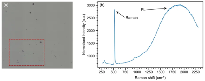
Figure 2. Initial microscopic and spectroscopic interrogation of the silicon wafer. (a) White light image of the area analyzed on the wafer. (b) A spectrum recorded at 830 nm showing Raman and PL bands from the silicon. Image Credit: Edinburgh Instruments
The silicon wafer dataset contains interrelated information on strain, crystallinity, and emission efficiency that univariate analysis frequently overlooks; nevertheless, multivariate algorithms automatically extract these correlations, allowing for speedy and objective evaluation of big datasets.1
The first multivariate method used was PCA, a popular dimensionality reduction technique that compresses complex datasets while preserving the most significant patterns.2 To better grasp what this entails, consider the spectral image of the silicon wafer that is to be analyzed.
The image measured 236 by 230 pixels, for a total of 54,280 pixels, and each had a spectrum with 1650 datapoints (or dimensions). This is a massive amount of data, which is computationally expensive.
PCA addresses this issue by performing a linear transformation that outputs a small number of new variables, designed to maximize the variance from the original dataset, called principal components (PCs).
The Python script used in this study generates five PCs that explain the prominent Raman and PL modes of variation in the original image, along with loading vectors that display the bands contributing to the spectral variance.
The prior dataset's 1650 dimensions are reduced to five, and extraneous information is filtered out as noise. Each pixel in the image will thus have five PC scores (PC1-5), which can be spatially mapped to highlight the most significant spectral changes in the dataset.
In the silicon wafer image dataset, PC1 and PC3 displayed significant variations in the PL and Raman bands. Figure 3 shows the score maps and loading vector plots for both PCs.
A defect, represented by the blue ellipsoid in Figure 3a, was of particular interest for this analysis due to its significant difference in spectral response from the rest of the wafer. This region corresponds to the thin stripe visible in the wafer's white-light picture, as shown in the red box in Figure 2a.
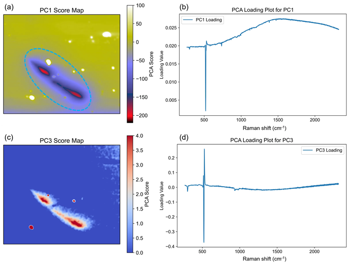
Figure 3. PCA imaging of the silicon wafer. (a) Score map and (b) loading vector plot for PC1. (c) Score map and (d) loading vector plot for PC3. Image Credit: Edinburgh Instruments
Figures 3a and 3b show the score map and loading plot for PC1. The loading figure indicates that PC1 captures the contrast between the silicon Raman and PL bands, with the Raman band at 520 cm-1 significantly negative and the PL band at 1900 cm-1 strongly positive.
As a result, positive PC1 scores indicate a dominant PL band, whereas low scores indicate attenuated PL in relation to the Raman band. The defect in the PC1 map is scored negatively (purple and red), indicating that the PL in this region is weaker relative to Raman scattering than in other regions on the wafer.
Figures 3c and 3d show the PC3 score map and loading point, respectively. The loading plot shows that PC3 captures only variations in the Raman signature of the silicon, with essentially no contribution from the PL band.
There are substantial negative and positive bands at 520 cm-1, indicating changes in the Raman band's peak position and/or form. This PC suggests that PL is reduced in the defect, possibly due to a Raman-shift-altering phenomenon like strain.
Overall, PCA shows that the highlighted flaw in the silicon wafer is associated with changes in the material's vibrational characteristics, leading to a drop in radiative emission.
While this structure-performance relationship can be detected by mapping and comparing Raman peak positions and PL intensities independently, multivariate analysis reveals these correlations directly and objectively, without the need for prior knowledge of which spectral features to study.
KMC Imaging of a Silicon Wafer for Simultaneous Raman and PL Analysis
KMC was also applied to the dataset to better visualize the spatial distribution of different spectral signatures over the silicon wafer. K-means is an unsupervised learning technique that divides datasets into 'k' clusters according to their similarity.3
In this article, it was used to group image pixels with similar Raman and PL spectral signatures into distinct spatial regions. It works by grouping pixels into clusters, minimizing the sum of squares within each cluster, and computing the mean spectrum for each cluster.
The 54,280 spectra in the silicon wafer image were clustered into 10 clusters using Python.
Each cluster was imaged discretely to reveal the wafer's heterogeneity in a way that the continuous colormaps used in PCA imaging did not. Figure 4a shows the KMC picture of the wafer.
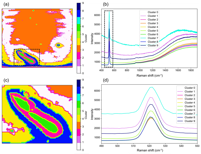
Figure 4. KMC imaging of the silicon wafer. (a) KMC image. (b) Mean spectra for each cluster. (c) Magnified view of the defect structure. (d) Magnified view of the Raman peak region. Image Credit: Edinburgh Instruments
Figure 4a's cluster image clearly delineates the previously observed defect structure, with Clusters 6 (green) and 3 (pink) highlighting significant inter-defect variation. Figure 4b highlights the mean spectra for each cluster.
Figures 4c and 4d show magnified images of the defect in the cluster image, as well as mean spectra focused solely on the Raman band.
The mean Raman shift from the green structure at the center of the defect is approximately 2 cm-1 lower than that of the surrounding pink structure. This research indicates that there is possibly tensile strain in the silicon within the flaw.
Similarly to PC1, the PL in the green cluster is lower than the outside defect and the rest of the wafer. The uniform reduction in PL with tensile strain demonstrates a clear relationship between structure and optoelectronic performance.
Conclusion
This article emphasizes the use of multivariate methods, particularly PCA and KMC, for analyzing complex Raman and PL spectra on silicon wafers.
These methods allow for efficient dimensionality reduction and pattern recognition, revealing subtle differences in strain and emission parameters that conventional univariate analysis would overlook.
Together, these tools provide a quick and dependable method for interpreting high-dimensional Raman and PL images.
Their use in Raman microscopy workflows improves material characterization and facilitates a better understanding of structure-property interactions in semiconductors. This method can improve wafer quality control, simplify defect identification, and offer faster feedback during semiconductor manufacturing.
References
- Zhang, C., et al. (2022). Strain Relaxation Effect on the Peak Wavelength of Blue InGaN/GaN Multi-Quantum Well Micro-LEDs. Applied Sciences, (online) 12(15), p.7431. DOI: 10.3390/app12157431. https://www.mdpi.com/2076-3417/12/15/7431.
- Ditta, A., et al. (2019). Principal components analysis of Raman spectral data for screening of Hepatitis C infection. Spectrochimica Acta Part A: Molecular and Biomolecular Spectroscopy, (online) 221, p.117173. DOI: 10.1016/j.saa.2019.117173. https://arrow.tudublin.ie/nanolart/98/.
- Xin, H., et al. (2022). Direct Detection of Inhomogeneity in CVD-Grown 2D TMD Materials via K-Means Clustering Raman Analysis. Nanomaterials, (online) 12(3), p.414. DOI 10.3390/nano12030414. https://www.mdpi.com/2079-4991/12/3/414.
- Higgs, V., et al. (2000). Photoluminescence characterization of defects in Si and SiGe structures. Journal of Physics: Condensed Matter, 12(49), pp.10105–10121. DOI: 10.1088/0953-8984/12/49/310. https://iopscience.iop.org/article/10.1088/0953-8984/12/49/310.

This information has been sourced, reviewed, and adapted from materials provided by Edinburgh Instruments.
For more information on this source, please visit Edinburgh Instruments.