In this interview, industry expert Angela Flack explains how multimodal microscopy, combining Raman, PL, and SHG techniques, enables comprehensive characterization of 2D materials for advanced research and technological innovation.
Can you start by explaining what multimodal microscopy is and how it applies to 2D materials research?
Multimodal microscopy combines multiple imaging and spectroscopic techniques within one platform to provide complementary information about a single sample. In the context of 2D materials, we typically integrate Raman spectroscopy, photoluminescence (PL), and second harmonic generation (SHG) imaging.
Each of these techniques probes a different physical property. Raman reveals lattice vibrations and phonon modes, PL explores electronic band structures, and SHG maps crystal symmetry. By combining these, we can fully characterize a material’s vibrational, optical, and structural features. This approach is essential for understanding layer number, defects, strain, and stacking orientation in Van der Waals materials.
What role does Raman spectroscopy play in characterizing 2D materials?
Raman spectroscopy uses monochromatic light to probe how photons interact with phonons in a material. Most of the scattered light is elastic, known as Rayleigh scattering, but a small fraction is inelastic. This inelastic scattering is the Raman signal, which gives us a fingerprint of the sample’s vibrational modes.
For 2D materials, Raman can determine the number of layers because the position, shape, and intensity of the Raman peaks vary strongly with layer thickness. It is also very effective for identifying defects, such as the D-band in graphene, monitoring strain, and mapping doping or chemical functionalization across a surface.
The RMS1000 system enables us to perform high-resolution Raman mapping quickly, using parameters such as a 532 nm laser and a 1800 grooves per mm grating to resolve subtle phonon shifts.
Can you describe how you set up and run a Raman map using the RMS1000?
Once we have located suitable flakes, such as molybdenum disulfide, typically on a silicon or sapphire substrate, we use bright field and dark field illumination to focus and select our mapping region. For 2D materials, we typically use a 532 nm laser because it gives a strong Raman signal with minimal fluorescence.
On the RMS1000, we select a high groove density grating to provide the spectral resolution required on these samples, such as 1800 gr/mm or 2400 gr/mm. Exposure times under 0.5 seconds enable what we call fast mapping, which significantly reduces total acquisition time from about six minutes to roughly ninety seconds. During mapping, we track the E2g and A1g Raman modes at approximately 385 and 405 inverse centimeters. Differences in their intensity or position reveal information about strain, layer number, and sample uniformity.
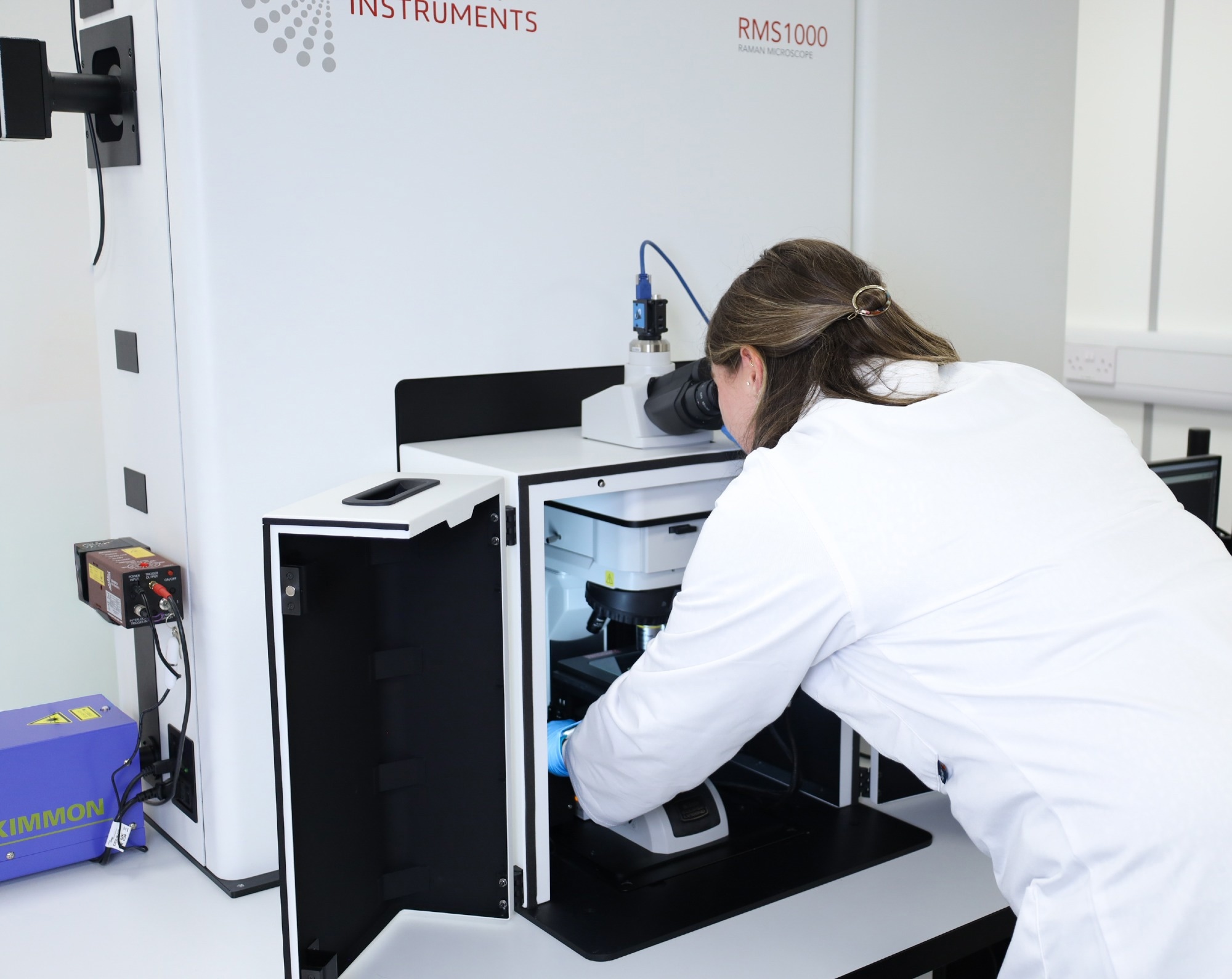
Image Credit: Edinburgh Instruments
How does photoluminescence imaging complement Raman spectroscopy in this workflow?
Photoluminescence, or PL, examines how a material emits light after absorbing it. When photons excite electrons to higher energy states, those electrons eventually recombine with holes, releasing energy as emitted photons. The wavelength of that emission reflects the electronic bandgap, giving us direct insight into the material’s electronic structure.
In PL mapping, we can visualize variations in layer number because PL intensity and peak position shift with thickness. It also helps detect defects and strain, and assess how surface modifications or the local environment affect optical behavior. It complements Raman spectroscopy because it provides information on electronic and optical properties rather than vibrational ones.
What are the main setup differences when running PL maps compared to Raman maps?
The workflow is very similar, but the measurement parameters change. PL is more sensitive, so we lower the laser power from 100 % to 20 % to prevent detector saturation or sample damage. We also use a low groove density grating, such as 300 gr/mm, because PL presents as broad emission bands instead of narrow peaks. We can still use the 532 nm laser, since visible excitation matches well with the band gaps of most 2D materials.
Using fast mapping again, we can collect a complete PL map in less than one minute. Interpreting the data is straightforward: higher PL intensity usually corresponds to monolayers, while red-shifted or weaker PL indicates multilayer or strained regions.
Can you explain second harmonic generation and why it is important for 2D materials?
Second harmonic generation, or SHG, is a nonlinear optical process where light of one frequency interacts with a non-centrosymmetric material to generate light at exactly twice that frequency. In simple terms, we shine a strong laser, for example, 1064 nm, onto a sample, and if the material lacks inversion symmetry, we detect emission at 532 nm.
SHG is highly sensitive to symmetry, so it allows us to determine stacking orientation in multilayer structures. For instance, monolayer molybdenum disulfide is non-centrosymmetric and produces a strong SHG signal, but certain bilayer configurations can restore symmetry, reducing or eliminating SHG. This makes it an ideal technique for mapping stacking order and twist angles in Van der Waals heterostructures.
How did you demonstrate SHG mapping on the RMS1000?
For SHG, we switched the excitation laser to 1064 nm and increased the power back to 100 percent. We still use fast mapping to visualize SHG intensity across the sample, and monitor the 532 nm peak.
The RMS1000 makes it easy to switch between Raman, PL, and SHG, allowing us to compare all three datasets over the same region directly. In our molybdenum disulfide example, we observed domains with varying SHG intensities that correspond to changes in crystal symmetry and stacking. The color maps revealed grain boundaries and distinct regions that were not visible in the Raman or PL data alone.
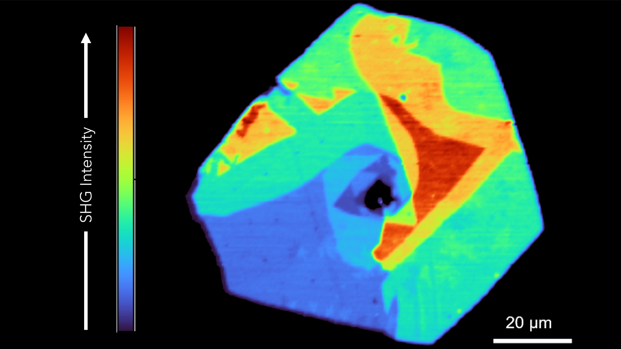
Image Credit: Edinburgh Instruments
You also analyzed tungsten diselenide. What insights did multimodal imaging reveal there?
Tungsten diselenide, or WSe2, is another 2D material with excellent electronic and optical properties. Using Raman, PL, and SHG together, we identified distinct regions corresponding to monolayer, bilayer, and trilayer areas. Raman helped us detect red-shifting of phonon modes and additional peaks that indicate multilayer stacking. PL confirmed this with varying intensities and peak shifts, showing stronger emission near 780 nm for monolayers and weaker, red-shifted peaks near 870 nm for thicker regions.
SHG then revealed stacking types. Three-R stacking increases SHG intensity, while two-H stacking introduces inversion symmetry and suppresses it. Combined, these techniques allowed us to map not only layer thickness but also symmetry and stacking configuration across the crystal.
How do these three techniques work together to build a complete picture of 2D materials?
When we combine Raman, PL, and SHG, we are effectively probing three different dimensions of the same material: vibrational, electronic, and structural. Raman provides information about lattice vibrations and phonon interactions. PL reveals details about the bandgap and electronic quality. SHG maps symmetry and stacking orientation.
Used together, they provide a comprehensive view of defects, strain, layer number, and overall crystal quality. It is a triple combination of spectroscopy that allows researchers to fully characterize and optimize 2D materials for applications in optoelectronics, sensing, and quantum technologies.
About Angela Flack 
Angela holds a Master’s degree in Analytical Chemistry from the University of Strathclyde. At Edinburgh Instruments, she has progressed from Application Specialist to Raman Product Manager. Drawing on her academic background and extensive experience in fluorescence and Raman spectroscopy, she supports product innovation and customer applications, combining strong analytical expertise with a deep understanding of advanced spectroscopic instrumentation.

This information has been sourced, reviewed, and adapted from materials provided by Edinburgh Instruments.
For more information on this source, please visit Edinburgh Instruments.
Disclaimer: The views expressed here are those of the interviewee and do not necessarily represent the views of AZoM.com Limited (T/A) AZoNetwork, the owner and operator of this website. This disclaimer forms part of the Terms and Conditions of use of this website.