Raman and photoluminescence microscopy are outstanding methods for characterizing, analyzing, and imaging gallium nitride (GaN)-based devices, as they can identify subtle alterations in the material’s crystalline structure.
- Gallium nitride (GaN) is a semiconductor with the potential to replace silicon in small, high-powered electrical devices thanks to its favorable thermal and electrical characteristics.
- Producers must monitor and ensure mechanical and electrical homogeneity throughout the manufacturing of GaN-based devices, as heterogeneity can compromise performance.
Gallium nitride (GaN) is a binary III/V semiconductor widely considered to be a promising alternative to silicon. It possesses a wider bandgap than silicon, allowing it to withstand higher voltages in electronic devices.1
Higher voltages enable GaN components to be smaller and more energy-efficient than silicon. In addition, GaN outperforms silicon during operation at elevated temperatures, helping to overcome current design limitations imposed by silicon technology in complex or challenging settings such as automobile electronics.2
In addition, GaN is widely used in the photonics sector, where it enables UV and blue light-emitting diodes (LEDs) and lasers. The development of these technologies set the stage for energy-efficient white LED lighting and led to Shuji Nakamura, Isamu Akasaki, and Hiroshi Amano receiving the 2014 Nobel Prize in Physics.
To achieve high-quality optoelectronic devices containing GaN, it is essential to minimize mechanical and electrical heterogeneity resulting from strain and crystal defects. Non-destructive analytical methods that are sensitive to these phenomena, such as Raman and photoluminescence (PL), are thus crucial for monitoring GaN throughout production.
This article showcases Raman and PL characterization and imaging of a GaN device using an Edinburgh Instruments RMS1000 Confocal Microscope. It demonstrates the sensitivity of both optical methods to even the most subtle material variations and shows that coupling them with a microscope enables spatial resolution of different material states.
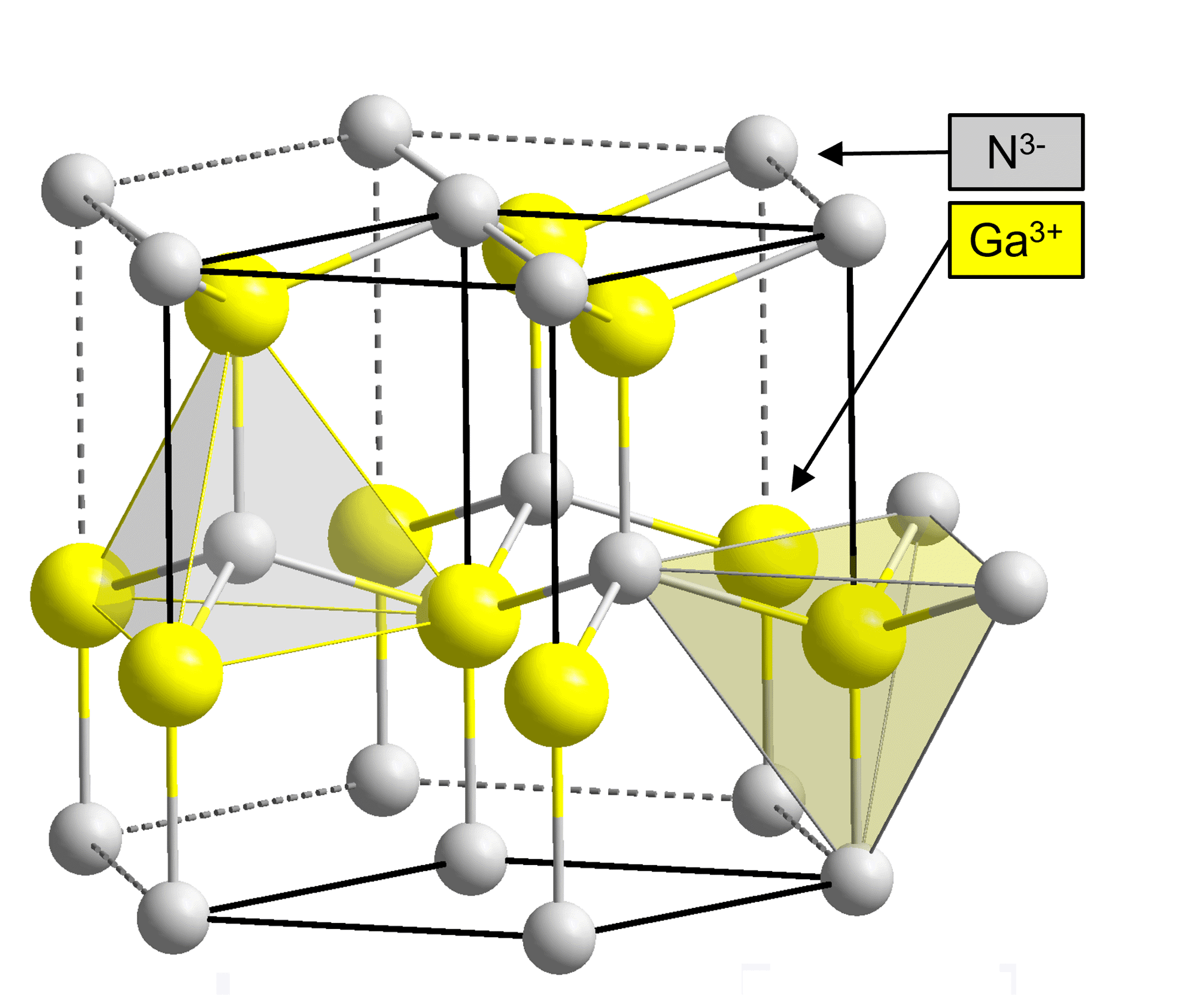
Figure 1. GaN Wurtzite crystal structure with the unit cell shaded yellow. Image Credit: Edinburgh Instruments
Materials and Methods
The evaluated samples were LED chips on an adhesive film manufactured by EPIGAP Optronic GmbH and engineered to emit at 520 nm. The LEDs were composed of GaN-based layers grown epitaxially on sapphire and Au alloy bonding pad electrodes.
An RMS1000 was configured with an externally coupled 325 nm He-Cd laser for PL characterization, a 638 nm laser for Raman characterization, and a CCD camera in a 225 mm spectrograph (Figure 2).
A 40X 0.47 NA UV objective lens was used when probing the sample with the 325 nm laser, and a 100X 0.9 NA objective lens was employed for the 638 nm evaluation. Automated X, Y, and Z stages enabled imaging with both spectroscopic methods.
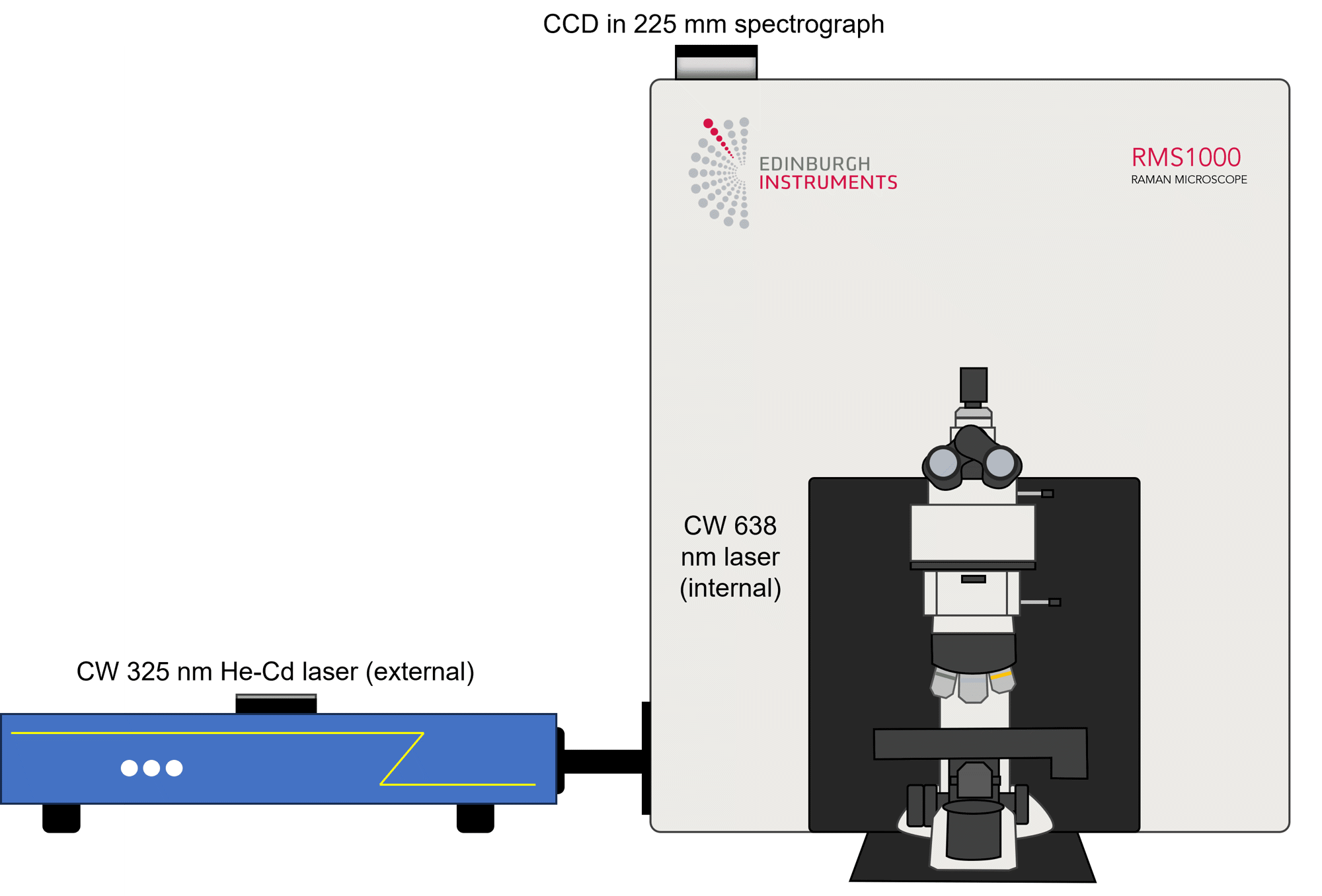
Figure 2. RMS1000 Confocal Microscope used for PL and Raman characterization of GaN. Image Credit: Edinburgh Instruments
Raman Characterization of GaN
First, Raman microscopy was employed to investigate the GaN LED chip. The Raman spectrum shown in Figure 3 highlights the two primary GaN bands in red. These are the E2 band at 567 cm-1 and the A1 longitudinal optical (LO) phonon at 735 cm-1.3
A peak at 670 cm-1 was also detected, which Cardoso et al. previously attributed to a disorder-activated vibrational mode of GaN.4 In addition, Raman bands from the underlying sapphire substrate (Al2O3) were observed at 420 cm-1 and 750 cm-1.
The characteristic PL signature from Cr3+ doped Al2O3 was observed at approximately 1300 cm-1, which corresponds to roughly 1.786 eV (694 nm).5
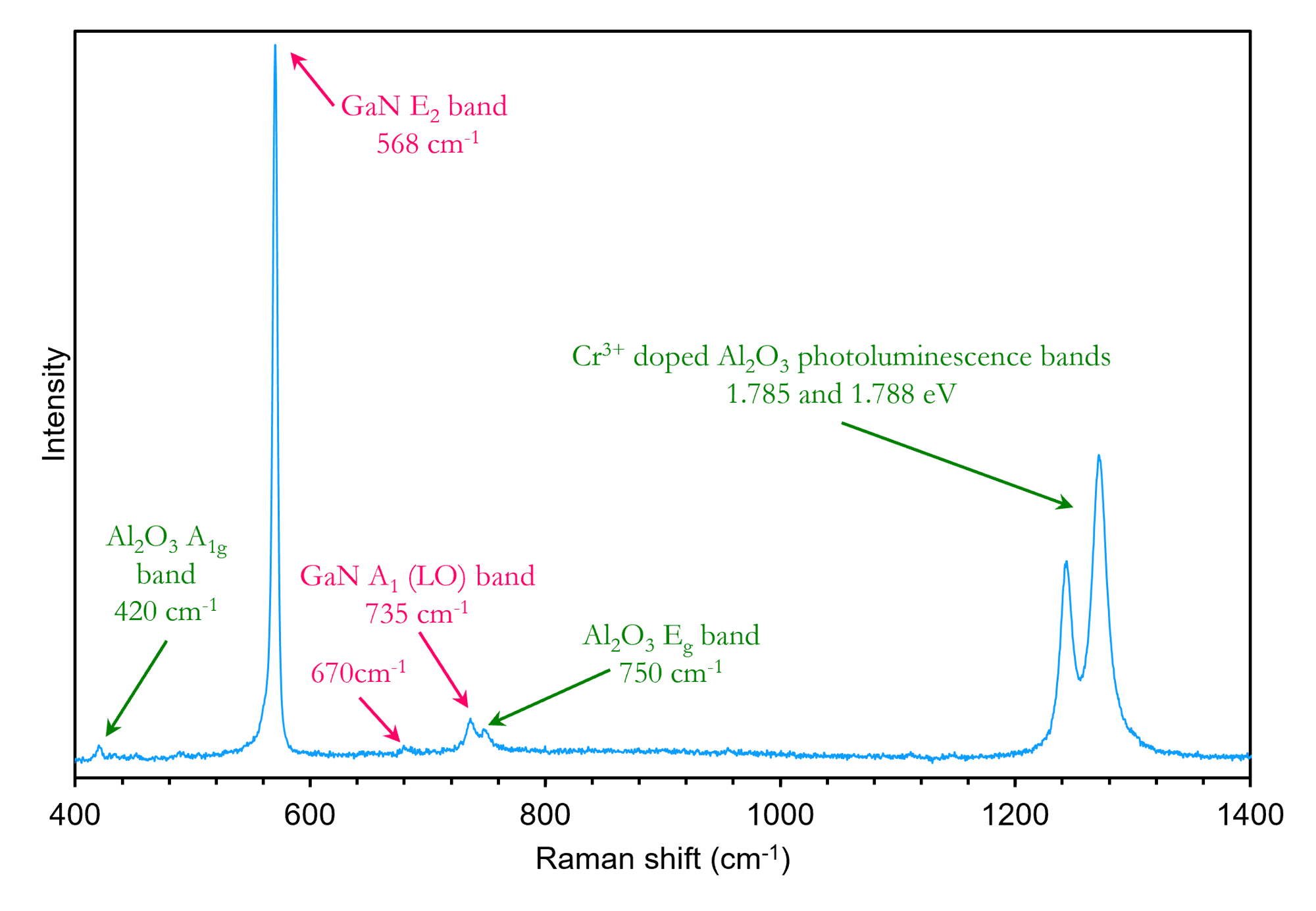
Figure 3. Raman spectrum of GaN. Image Credit: Edinburgh Instruments
A region of the GaN chip was imaged using spectral mapping with the 638 nm laser. Imaging of the E2 (high) mode was carried out to determine GaN distribution within this region, as shown in Figure 4b. The results show that the intensity remained consistently higher in the area of the chip within the P- and N-GaN layers.
Figure 4c illustrates the mapping of the E2 (high) mode position. The Raman shift of this mode can be correlated with strain in GaN, where an increase in Raman shift relative to 567 cm-1 indicates compressive strain, while a decrease indicates tensile strain. Raman microscopy can readily visualize strain on semiconductor materials such as GaN and silicon.
In the image in Figure 4c, areas where the GaN is experiencing compressive strain are indicated by yellow and red regions, while areas of tensile strain are represented by the black regions. The spectra in Figure 4d illustrate the fluctuation in intensity and peak position of the GaN E2 band across the images.
The sapphire PL intensity was also imaged in Figure 4e, with corresponding spectra in Figure 4f, demonstrating that the sapphire PL was diminished in the areas exhibiting the strongest GaN Raman intensity.
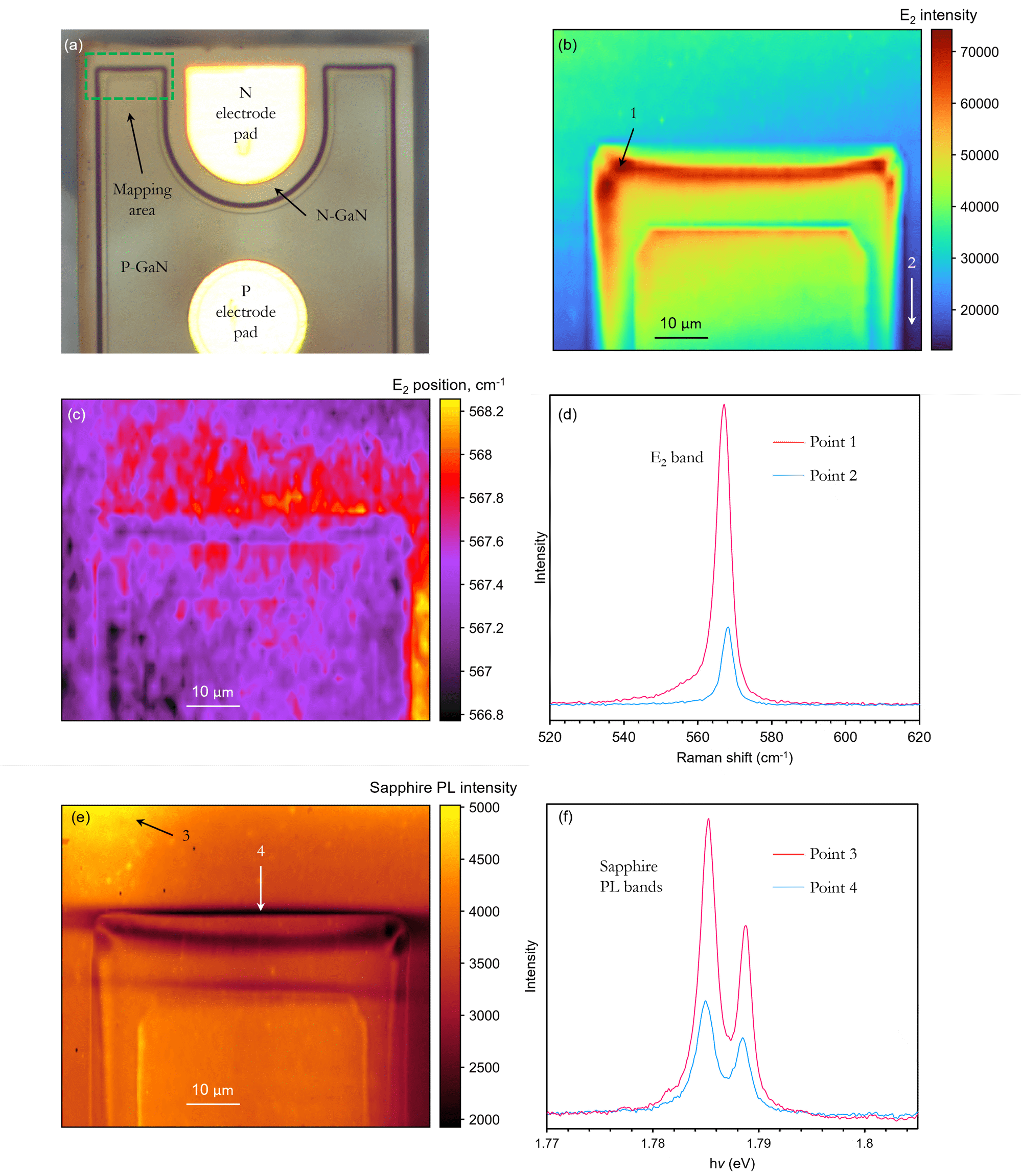
Figure 4. Raman mapping of GaN. Image Credit: Edinburgh Instruments
Photoluminescence Characterization of GaN
PL microscopy, which directly measures bandgaps in semiconductor materials, was used to evaluate the GaN chip. Since bandgap energies are highly sensitive to impurities such as dopants and defects, microscopic evaluation of devices can provide information about their presence.
As shown in Figure 5, the PL spectrum of GaN at ambient temperature is dominated by a strong near-band-edge (NBE) emission at 3.41 eV (364 nm), correlating to the direct band-to-band recombination between electrons in the conduction band and holes in the valence band (see Figure 4).6
A 325 nm He-Cd laser was externally coupled to the RMS1000 to excite and observe this band. PL bands at 2.33 eV (532 nm) and 1.71 eV (725 nm) were also observed in the spectrum. The sapphire PL band was not detected, most likely due to the greater absorption coefficient of the surface GaN material upon application of the 325 nm UV excitation wavelength.
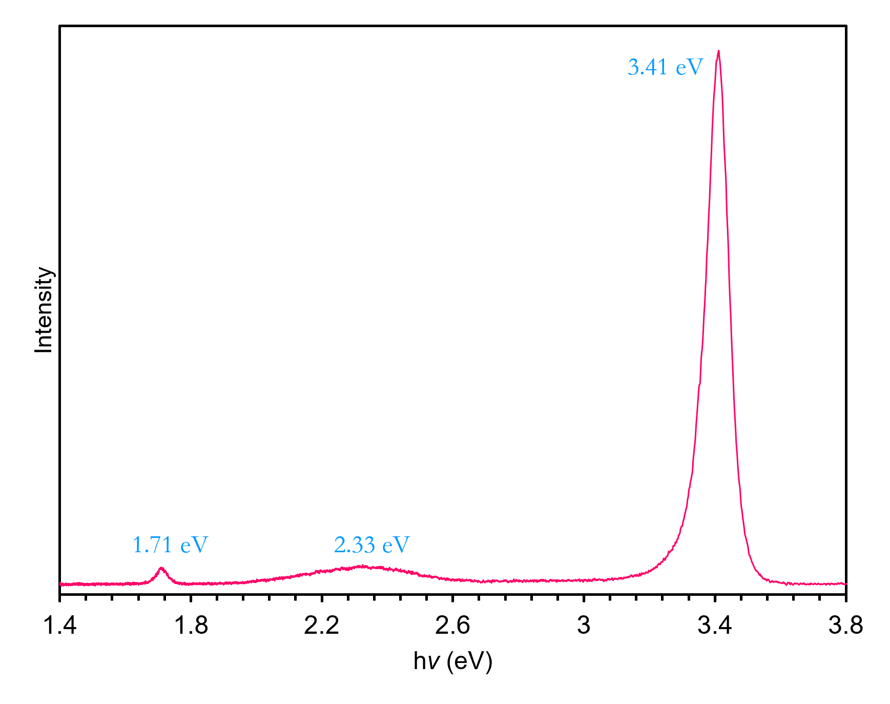
Figure 5. Photoluminescence spectrum of GaN. Image Credit: Edinburgh Instruments
PL imaging was carried out on the same chip region examined with Raman, as shown in Figure 6. The full area displayed in Figure 6a was visualized in brightfield using the UV objective, followed by false color imaging via UV and visible bands, as shown in Figures 6b and 6c. The 3.41 eV NBE UV PL intensity image reveals that the chip’s P-GaN region exhibits no PL.
Hess et al. previously examined the effect of diminishing NBE PL of GaN with increasing Mg dopant concentration (P doping).7 The N-GaN region emits strong UV PL, with the exception of an area in the top right-hand side of the image. The Raman image in Figure 4c showed that this area was under compressive strain.
Additionally, the chip emitted at 2.38 eV (520 nm), corresponding to the PL from the InGaN layer, which is located between P- and N-GaN and is responsible for the green color of the LED. The emission in this area was more intense and blue-shifted from the weak visible emissions in the N-GaN layer.
This emission was mostly confined to the black strip located at the boundary of the P and N layers. Figure 6d shows the UV and green PL spectra from points 1 and 2 on both maps.
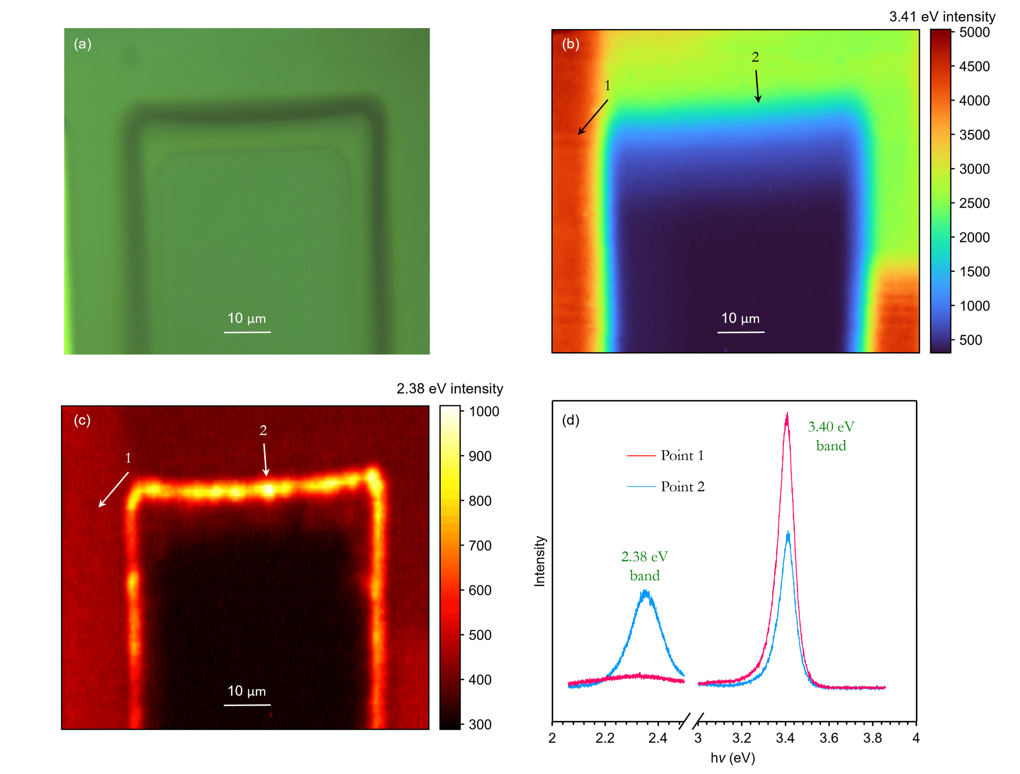
Figure 6. PL mapping of GaN. Image Credit: Edinburgh Instruments
Conclusion
The RMS1000 Raman and PL Confocal Microscope is ideally suited for analyzing and characterizing GaN-based devices. By combining Raman and PL methods, it was possible to visualize differences in the crystalline structure and chemical composition of the constituent materials across the chip. Both of these methods are highly beneficial for the non-destructive quality control monitoring of GaN-based devices.
References and Further Reading
- Davis, R.F., et al. (1988). Critical evaluation of the status of the areas for future research regarding the wide band gap semiconductors diamond, gallium nitride and silicon carbide. Materials Science And Engineering: B, 1(1), pp.77–104. DOI:10.1016/0921-5107(88)90032-3. https://www.sciencedirect.com/science/article/abs/pii/0921510788900323?via%3Dihub.
- Kim, N.-I., et al. (2020). Piezoelectric pressure sensor based on flexible gallium nitride thin film for harsh-environment and high-temperature applications. Sensors and Actuators A: Physical, 305, p.111940. DOI:10.1016/j.sna.2020.111940. https://www.sciencedirect.com/science/article/abs/pii/S0924424719320710?via%3Dihub.
- Kuball, M. (2001). Raman spectroscopy of GaN, AlGaN and AlN for process and growth monitoring/control. 31(10), pp.987–999. DOI:10.1002/sia.1134. https://analyticalsciencejournals.onlinelibrary.wiley.com/doi/10.1002/sia.1134.
- Cardoso, J., et al. (2021). Exploring swift-heavy ion irradiation of InGaN/GaN multiple quantum wells for green-emitters: the use of Raman and photoluminescence to assess the irradiation effects on the optical and structural properties. Journal of Materials Chemistry C, 9(28), pp.8809–8818. DOI:10.1039/D1TC01603B. https://pubs.rsc.org/tc/article/9/28/8809/752963/Exploring-swift-heavy-ion-irradiation-of-InGaN-GaN.
- Liu, D., et al. (2012). Al2O3:Cr3+ microfibers by hydrothermal route: Luminescence properties. Materials Research Bulletin, 47(9), pp.2332–2335. DOI:10.1016/j.materresbull.2012.05.026. https://www.sciencedirect.com/science/article/abs/pii/S0025540812004023?via%3Dihub.
- Santana, G., et al. (2013). Photoluminescence Study of Gallium Nitride Thin Films Obtained by Infrared Close Space Vapor Transport. Materials, 6(3), pp.1050–1060. DOI:10.3390/ma6031050. https://www.mdpi.com/1996-1944/6/3/1050.
- Hess et al., Photoluminescence Studies of Mg-Doped and Si-doped Gallium Nitride Epilayers, Physica Status Solidi B, 1998, 210, 465-470.

This information has been sourced, reviewed, and adapted from materials provided by Edinburgh Instruments.
For more information on this source, please visit Edinburgh Instruments.