Gallium nitride (GaN) has emerged as a key material in the semiconductor industry, with substantial benefits over older silicon-based technologies.
- Gallium nitride (GaN) is a promising semiconductor material that outperforms silicon-based devices. However, optimal performance requires high-quality GaN.
- Photoluminescence (PL) spectroscopy is a non-destructive method for evaluating GaN quality by analyzing emission properties and detecting defects.
- Measuring steady-state and time-resolved PL in GaN helps distinguish between intrinsic characteristics and defect-related emissions, providing vital insights into material quality.
GaN is a binary III/V semiconductor with a direct bandgap of around 3.4 eV, which is roughly three times that of silicon (1.1 eV).1,2
GaN's broad bandgap enables it to withstand high electric fields, resulting in smaller, more efficient power electronics capable of handling high voltages and currents. GaN's large bandgap enables electroluminescence in the near-UV to blue range, making it ideal for UV and blue light-emitting diodes (LEDs) and lasers.3
Other advantageous characteristics of GaN are its endurance, excellent conductivity, and high heat capacity. These properties make GaN an excellent contender for high-voltage and high-temperature transistors in applications such as wireless communication infrastructure and aeronautical technology.
It is key to ensure that GaN materials are of high quality, with minimal mechanical and electrical heterogeneity caused by strain and crystal flaws. Photoluminescence (PL) provides a sensitive, non-destructive method for evaluating the quality of GaN materials.
When defects are present in the material, defect-induced energy levels with reduced band gaps form, leading to radiation emission at various wavelengths.4 Common GaN faults cause luminescence in the yellow range.
Time-resolved PL measurements provide additional information on the quality of GaN materials. GaN has very short PL lifetimes in the picosecond to nanosecond range. In contrast, faults often have longer lives, ranging from microseconds to seconds.4
This article shows how to use an Edinburgh Instruments FLS1000 Photoluminescence Spectrometer with an external picosecond pulsed UV laser to perform steady-state and time-resolved PL studies of GaN.
Materials and Methods
An FLS1000 was used for measurements, which included an externally connected 266 nm picosecond pulsed laser (PS-D-266_Air_A_10mW, CNI Laser) and a high-speed hybrid-PMT detector (HS-HPD) (Figure 1).
The sample under investigation was an undoped n-type GaN on a sapphire substrate, grown by halide vapor-phase epitaxy (HVPE).
The sample was placed in a front-face sample holder, with a 325 nm longpass filter inserted before the emission monochromator to eliminate laser scattering because the sample was reflective.
Time-resolved PL measurements of GaN were obtained utilizing time-correlated single photon counting (TCSPC) at a laser repetition rate of 500 kHz. The GaN flaws were detected using multichannel scaling (MCS) with a microsecond xenon flashlamp at a 100 Hz repetition rate.
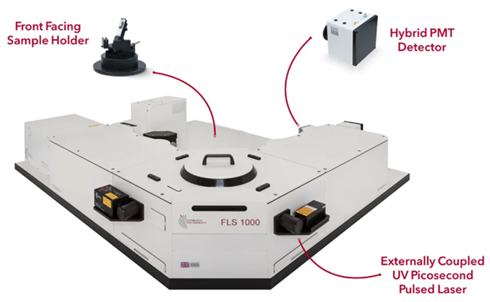
Figure 1. FLS1000 spectrometer with an externally coupled 266 nm laser, front-facing sample holder, and hybrid PMT detector used for PL measurements of GaN. Image Credit: Edinburgh Instruments
Stable State PL of GaN
PL spectroscopy is an effective method for estimating energy gaps, especially in wide-bandgap semiconductors such as GaN.
Figure 2 shows the emission spectrum of GaN, which includes a peak at 365 nm corresponding to a bandgap energy of 3.4 eV. This peak is due to band-edge emission from GaN, resulting from direct band-to-band recombination between electrons in the conduction band and holes in the valence band.
In addition, a wider luminescence band at roughly 550 nm (2.25 eV) was found, indicating defect-related emission in the GaN. This luminescence defect in the material is frequently linked to gallium vacancy-related defects.
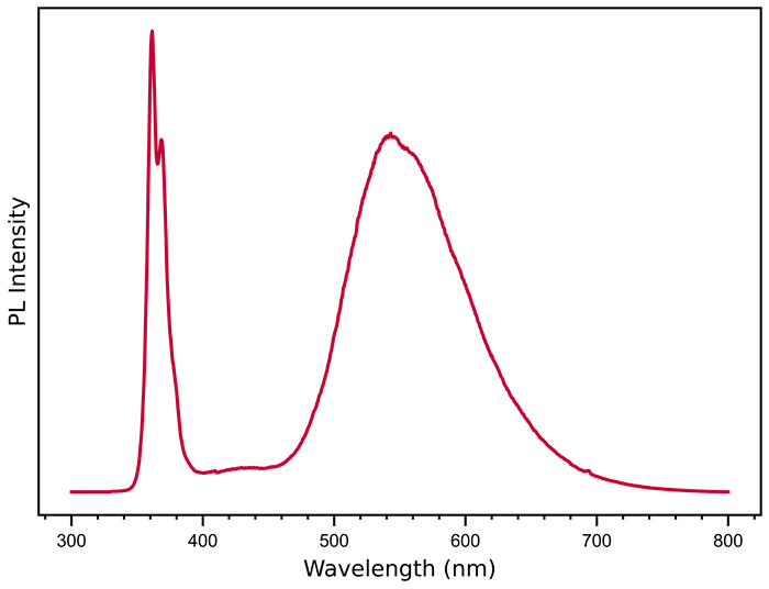
Figure 2. Emission spectrum of GaN. Measurement parameters: λex = 266 nm, Δλem = 1 nm, step = 0.5 nm, dwell time = 1 s. Image Credit: Edinburgh Instruments
PL Lifetime of GaN
PL lifetimes were measured at 370 and 550 nm, corresponding to GaN and flaws, respectively. The PL lifetime of the GaN band-edge emission at 370 nm was measured with TCSPC.
The instrument response function (IRF) was assessed at the laser wavelength (266 nm). Figure 3 shows the fluorescence degradation, IRF, and calculated lifespan.
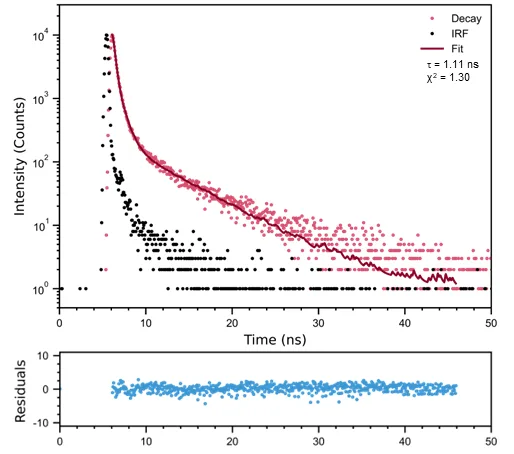
Figure 3. Fluorescence decay and calculated PL lifetime of GaN at 370 nm emission. Measurement parameters: λex = 266 nm, Δλem = 1 nm, repetition rate = 500 kHz. Image Credit: Edinburgh Instruments
The decay was fitted by reconvolving the IRF with the sample's exponential decay. The photoluminescence decay was fitted with a three-component exponential function, yielding relaxation times of 0.26, 0.77, and 5.78 ns. This resulted in an intensity average lifetime of 1.11 ns.
The PL lifetime of the defect emission at 550 nm was also determined using MCS single-photon counting and a microsecond xenon flashlamp excitation source (Figure 4).
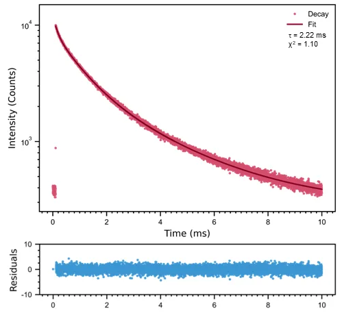
Figure 4. Fluorescence decay and calculated PL lifetime of GaN at 550 nm emission. Measurement parameters: λex = 365 nm, Δλex = 1 nm, Δλem = 3 nm, repetition rate = 100 Hz. Image Credit: Edinburgh Instruments
The decay was fitted with a three-component exponential, yielding relaxation times of 141.2, 915.2, and 2906.8 µs, with an average intensity lifespan of 2.22 ms.
The prolonged lifetimes in the microsecond-to-second range were characteristic of GaN faults, suggesting that this technique was useful for analyzing the quality of GaN materials.
Conclusion
The FLS1000 spectrometer, in combination with an external UV laser, enabled the measurement of GaN's steady state and time-resolved PL. The steady-state PL spectra revealed emission bands characteristic of crystalline GaN and GaN with structural flaws.
Time-resolved PL measurements of these emission bands supported this. The combination of steady-state and time-resolved PL analysis is an effective method for determining GaN quality.
References
- Davis, R.F., et al. (1988). Critical evaluation of the status of the areas for future research regarding the wide band gap semiconductors diamond, gallium nitride and silicon carbide. Materials Science And Engineering: B, 1(1), pp.77–104. DOI: 10.1016/0921-5107(88)90032-3. https://www.sciencedirect.com/science/article/abs/pii/0921510788900323.
- Santana, G., et al. (2013). Photoluminescence Study of Gallium Nitride Thin Films Obtained by Infrared Close Space Vapor Transport. Materials, 6(3), pp.1050–1060. DOI: 10.3390/ma6031050. https://www.mdpi.com/1996-1944/6/3/1050.
- Nakamura, S., Mukai, T. and Senoh, M. (1991). High-Power GaN P-N Junction Blue-Light-Emitting Diodes. Japanese Journal of Applied Physics, 30(Part 2, No. 12A), pp.L1998–L2001. DOI: 10.1143/jjap.30.l1998. https://iopscience.iop.org/article/10.1143/JJAP.30.L1998.
- Reshchikov, M.A. and Morkoç, H. (2005). Luminescence properties of defects in GaN. Journal of Applied Physics, 97(6), p.061301. DOI: 10.1063/1.1868059. https://pubs.aip.org/aip/jap/article-abstract/97/6/061301/984603/Luminescence-properties-of-defects-in-GaN?redirectedFrom=fulltext.

This information has been sourced, reviewed, and adapted from materials provided by Edinburgh Instruments.
For more information on this source, please visit Edinburgh Instruments.