Multimodal imaging with a single instrument and a single software platform enables comprehensive characterization of layer-dependent optoelectronic attributes in 2D materials.
- Raman imaging can be used to resolve monolayer and multilayer WSe2.
- Photoluminescence imaging probes multilayer crystal areas that contain bilayer and trilayer WSe2 regions.
- Second harmonic generation imaging determines layer orientation of multilayer WSe2.
Two-dimensional transition-metal dichalcogenides represent a category of layered semiconducting materials that display distinct optical and electronic characteristics that depend on layer number.
This article explores the capability of the RMS1000 Confocal Microscope for multimodal imaging of tungsten diselenide (WSe2). The microscope includes five multimodal imaging options: reflected brightfield and darkfield, Raman, photoluminescence, and second harmonic generation to fully characterize its layer-dependent optoelectronic attributes.
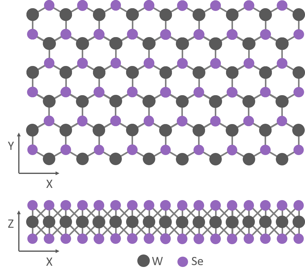
Figure 1. Monolayer WSe2 Crystal Structure. Image Credit: Edinburgh Instruments
Materials and Methods
Chemical vapor deposition (CVD) was used to grow WSe2 crystals on a Si substrate, which were then characterized with an Edinburgh Instruments RMS1000 Confocal Microscope. The RMS1000 included a 100x NA 0.9 objective and a back-illuminated CCD camera.
The WSe2 was excited using a 532 nm laser for both Raman and photoluminescence imaging. An 1800 gr/mm diffraction grating was used to acquire the Raman spectra, while a 300 gr/mm diffraction grating was used to collect photoluminescence spectra.
For second harmonic generation (SHG) imaging, a Chromacity 1040 HP femtosecond fiber laser (Chromacity Ltd., UK) operating at 1040 nm and 80 MHz was coupled to the RMS1000 for excitation. A 300 gr/mm diffraction grating was employed to acquire the SHG response.
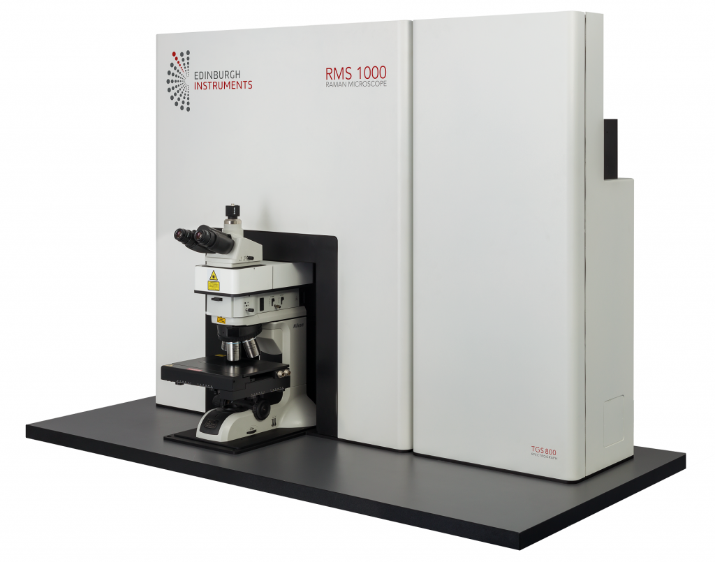
Figure 2. Edinburgh Instruments RMS1000 Multimodal Confocal Microscope. Image Credit: Edinburgh Instruments
Reflected Brightfield and Darkfield Imaging
Initial widefield imaging of the WSe2 crystal was carried out using reflected brightfield and darkfield, as shown in Figure 3. The reflected brightfield image shows the reflective silicon substrate as bright and the absorbing WSe2 crystal deposited atop as darker. Dark spots across the crystal surface correspond to nucleation sites, while the stronger absorbing domain in the center indicates multilayer WSe2.
Complementary information is obtained through reflected darkfield imaging. In darkfield, the sample is illuminated at an oblique angle, and steps in sample surface height generate greater scattering, appearing bright in the image. The darkfield image shows two areas in the central domain with differing heights, most probably due to different WSe2 layer numbers.
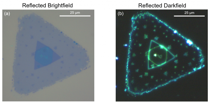
Figure 3. (a) Reflected brightfield and (b) reflected darkfield imaging of the WSe2 crystal. Image Credit: Edinburgh Instruments
Raman Imaging
The crystal was subsequently imaged using Raman (Figure 4). WSe2 exhibits a characteristic Raman peak at 250 cm-1 (Figure 4d) corresponding to the in-plane E12g and out-of-plane A1g phonon modes of WSe2.
Unlike other transition-metal dichalcogenides, the E12g and A1g phonon modes are nearly degenerate in WSe2 and are not individually resolved, with both contributing to the 250 cm-1 peak.1,2
In the crystal center, an additional peak at 310 cm-1 is detected (marked with arrows in Figure 4d). This peak is symmetry-forbidden in monolayer WSe2 and indicates multilayer WSe2.2
The E12g/A1g peak intensity shown in Figure 4a is strongest in the large primary triangle domain and decreases by approximately 80% within the inner triangle domain. This decrease in intensity indicates a transition from monolayer to multilayer WSe2.1
As shown in Figure 4b, the E12g/A1g peak position shifts from 250 cm-1 in the primary domain to 247 cm-1 within the inner domain, supporting a change in layer number.3 This peak also shifts towards higher wavenumbers at the crystal edges, which is attributed to variations in the local microenvironment at the disordered edges.
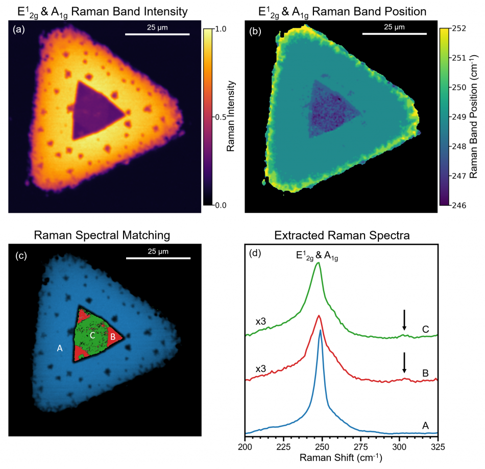
Figure 4. Raman imaging of WSe2. (a) Intensity of the E12g / A1g (250 cm-1) Raman band, (b) peak position of the E12g / A1g Raman band, (c) least squares spectral matching revealing three distinct Raman spectral areas, (d) averaged Raman spectra from areas A, B, and C; spectra B and C are scaled in intensity by a factor of three and the arrows mark the location of the multilayer 310 cm-1 peak. The Raman imaging parameters were: 40 x 40 μm2, 200 x 200 pixels, 50 ms integration time, 532 nm laser, 1800 gr/mm diffraction grating, 300 μm pinhole.
Ramacle® spectral matching analysis (Figure 4c) identified three distinct Raman spectral regions in the crystal. In spectral matching, spectra at user-selected locations in the map are designated as archetypes, and the deviation of all other spectra in the map from the archetype is calculated. Lower deviations from the archetype spectra are represented by more intense color.
The monolayer WSe2 primary domain is highlighted in blue, while the inner domain was found to be composed of two regions (highlighted in red and green) with subtly different E12g / A1g Raman peak shapes. This agrees with the change in surface height in the inner domain observed in the darkfield image. Image Credit: Edinburgh Instruments
Photoluminescence Imaging
The crystal was photoluminescence (PL) imaged to gain further insight into the inner domain (Figure 5). The total PL intensity (Figure 5a) is lower within the inner domain, and the PL peak position (Figure 5b) is red-shifted.
Spectral matching (Figure 5c) revealed four distinct PL spectral areas across the crystal, with their corresponding spectra displayed in Figure 5d.
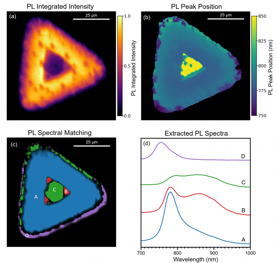
Figure 5. Photoluminescence imaging of WSe2. (a) Integrated intensity of the PL response, (b) PL primary peak position, (c) least squares spectral matching revealing four distinct PL spectral areas, (d) averaged PL spectra from areas A, B, C and D. The PL imaging parameters were: 40 x 40 μm2, 200 x 200 pixels, 30 ms integration time, 532 nm laser, 300 gr/mm diffraction grating, 300 μm pinhole.
Region A (blue) is monolayer WSe2 with a PL peak at 780 nm from confined exciton emission. In region B, the total PL intensity is decreased with a longer-wavelength shoulder peak at 870 nm, while in region C the PL intensity decreases further and spectral weight shifts to the long-wavelength shoulder. It has been established that as the number of layers increases in WSe2, the PL emission red-shifts from exciton-based emission at ~1.6 eV (~780 nm) in the monolayer to indirect bandgap emission at ~1.2 eV (~1000 nm) in bulk WSe2.1
Regions B and C are therefore assigned as bilayer and trilayer WSe2, respectively. Similarly to the Raman image, significant edge effects were also observed in the PL, with the PL peak position blue-shifted on the lower edge (spectrum D) and red-shifted on the upper edge of the crystal. Image Credit: Edinburgh Instruments
Second Harmonic Generation Imaging
The crystal was imaged using second harmonic generation (SHG) to determine the layer orientation within the three identified domains (Figure 6). SHG imaging exhibits high sensitivity to the crystalline symmetry of transition metal dichalcogenides, as SHG occurs only when the excitation focal volume contains a non-centrosymmetry.
Monolayer WSe2 is non-centrosymmetric, and region A contains a measurable SHG response, as anticipated.
The symmetry of multilayer WSe2 is determined by the layer stacking type, either 2H or 3R.5 In 3R stacking, all layers possess the same orientation and the multilayer is non-centrosymmetric, with the SHG response increasing according to layer number.
Conversely, 2H stacking involves a 180 ° rotation of each layer relative to the adjacent layers. Odd-numbered multilayers are net non-centrosymmetric and exhibit an SHG response comparable to that of the monolayer, whereas even-numbered multilayers are net centrosymmetric without a SHG response.4,5
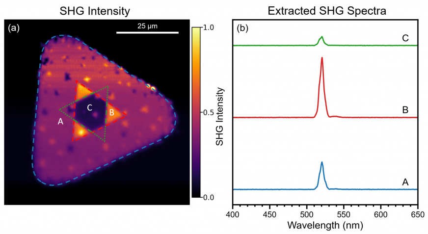
Figure 6. Second harmonic generation imaging of WSe2. (a) Intensity of the SHG peak at 520 nm. (b) Extracted SHG response from areas A, B, and C. The SHG imaging parameters were: 40 x 40 μm2, 200 x 200 pixels, 11 ms integration time, 1040 nm femtosecond pulsed laser, 300 gr/mm diffraction grating, 300 μm pinhole.
The bilayer WSe2 in region B has an SHG response that is twice that of the monolayer, and the two layers therefore must be 3R stacked. The trilayer WSe2 in region C has a diminished SHG response compared to the monolayer, which indicates the third layer in the trilayer is rotated relative to the first and second layers, resulting in a partial restoration of centrosymmetry.
The blue, red, and green dashed triangles in Figure 6a illustrate the relative orientations of the three layers in the crystal. The growth of the third layer (green) has terminated at the boundaries of the second layer (red), resulting in a partial triangle. Image Credit: Edinburgh Instruments
Conclusion
By combining widefield, Raman, PL, and SHG imaging methods, the layer number and stacking type in a CVD-grown WSe2 crystal were determined. Thanks to its multimodal imaging abilities, the RMS1000 Confocal Microscope is an effective imaging platform for investigating the optoelectronic characteristics of transition-metal dichalcogenides.
References and Further Reading
- Tonndorf, P., et al. (2013). Photoluminescence emission and Raman response of monolayer MoS2, MoSe2, and WSe2. Optics Express, 21(4), 4908. DOI:10.1364/oe.21.004908. https://opg.optica.org/oe/fulltext.cfm?uri=oe-21-4-4908
- Ribeiro-Soares, J., et al. (2015). Second Harmonic Generation in WSe2. 2D Materials, 2(4), 045015. DOI:10.1088/2053-1583/2/4/045015. https://iopscience.iop.org/article/10.1088/2053-1583/2/4/045015.
- Terrones, H., et al. (2014). New First Order Raman-active Modes in Few Layered Transition Metal Dichalcogenides. Scientific Reports, 4(1). DOI:10.1038/srep04215. https://www.nature.com/articles/srep04215.
- Zhao, M., et al. (2016). Atomically phase-matched second-harmonic generation in a 2D crystal. Light: Science & Applications, 5(8), e16131–e16131. DOI:10.1038/lsa.2016.131. https://www.nature.com/articles/lsa2016131.
- Shinde, S. M., et al. (2018). Stacking-controllable interlayer coupling and symmetric configuration of multilayered MoS2. NPG Asia Materials, 10(2), e468–e468. DOI:10.1038/am.2017.226. https://www.nature.com/articles/am2017226.

This information has been sourced, reviewed, and adapted from materials provided by Edinburgh Instruments.
For more information on this source, please visit Edinburgh Instruments.