Organic light-emitting diode (OLED) displays are created using arrays of self-emissive subpixels. Individual subpixels are reaching the micron scale, but their collective luminance and spectral behavior determine a display's lifetime, uniformity, and perceived color accuracy.
Traditional colorimeters and spectroradiometers average light over a spot size much larger than a single subpixel, meaning that they cannot be used to characterize OLED emission at the feature scale required for current high-pixel-density panels.
Microspectrophotometry (MSP) setups integrate an optical microscope with a spectrophotometer, closing this capability gap by enabling full spectral measurement from micron-scale sample areas.
This article examines the operating principle of microspectrophotometers, explores their role in OLED research and development and production quality control through a series of real-world application examples, and outlines the varied benefits of MSP compared with alternative measurement techniques.
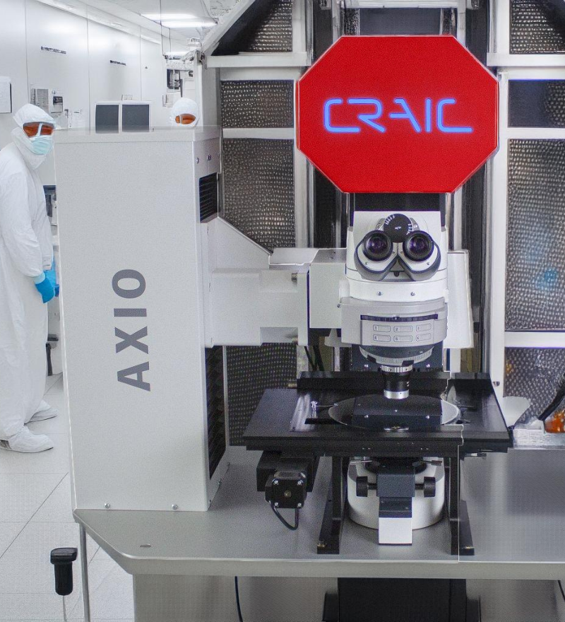
Figure 1. The 2030XL PRO™ is a microspectrophotometer designed to measure large-form-factor flat-panel displays with micron-scale spatial resolution. Image Credit: CRAIC Technologies
A microspectrophotometer integrates a custom-built microscope’s UV-Visible-NIR range optics and light sources and an optimized spectrophotometer. This novel approach allows acquisition of a full spectral-range signature from a spatially defined region of a sample, as small as a few microns in diameter. The signature is acquired using either reflectance, transmittance, or emission intensity as a function of wavelength.
The ‘sample’ of interest in an OLED context is generally a single subpixel, a small region of a finished panel, a defect site, or a thin-film stack on a test coupon.
OLED displays consist of stacked organic layers (hole-injection, hole-transport, emissive, electron-transport, and electron-injection layers) sandwiched between electrodes. These displays leverage red, green, and blue (RGB) subpixels, with an occasional white or extra colored emitter, all patterned at the micron scale.
Each subpixel is an independent light source featuring its own spectral emission curve. This emission curve is sensitive to drive current, dopant concentration, layer thickness, temperature, and degradation state, meaning that engineers must be able to investigate emission spectra at the resolution of the specific pixel structure.
This need underpins the use of a microspectrophotometer, rather than a bulk optical measurement tool.
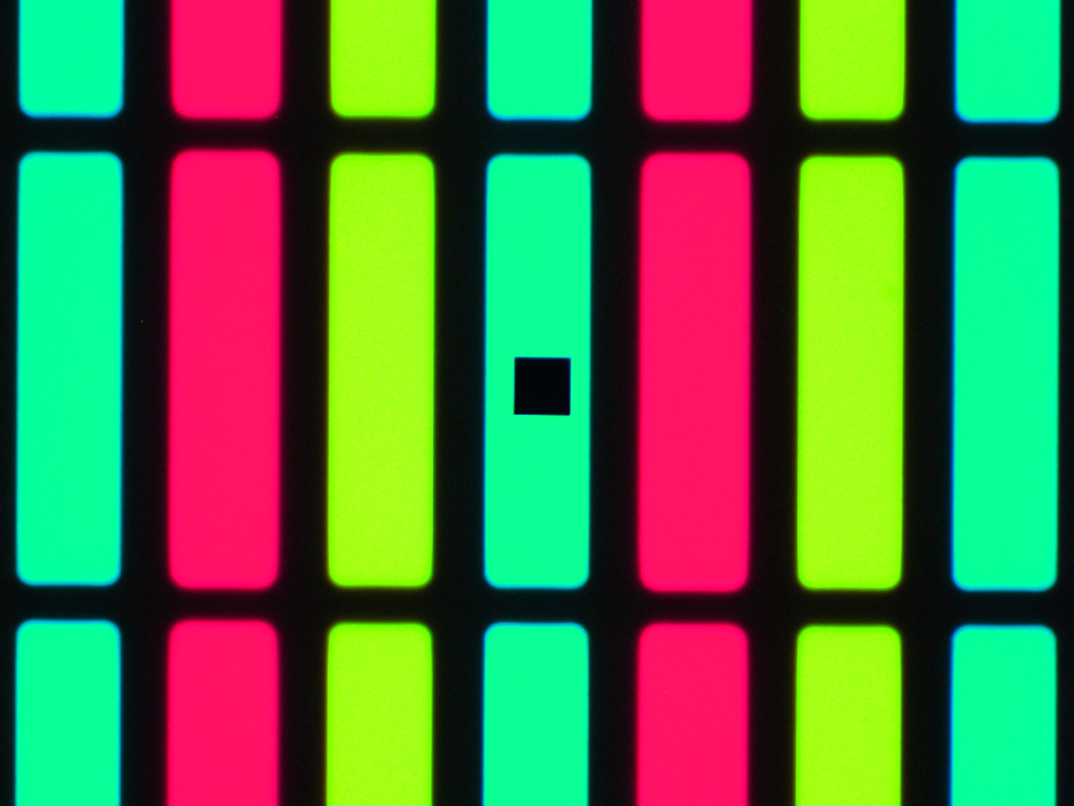
Figure 2. Red, yellow and green pixels sampled with a microspectrophotometer aperture size of only 10 micron2. The pixels are only 18 microns wide. Image Credit: CRAIC Technologies
Principle of Operation
A common MSP system used in display metrology comprises:
- Microscope optics featuring UV-visible-NIR range objective lenses (of various magnifications) designed to image the sample plane and define the specific measurement spot
- An aperture selection, including a fixed or variable aperture placed at an intermediate image plane to reject light from neighboring structures and precisely restrict the measured area to a single feature of interest or subpixel
- An illumination path for transmittance or reflectance work, featuring optics and a stabilized, calibrated light source like the Scorpii™ lighting system. This light source is used rather than using the OLED's own emission to enable characterization of color filters, passive optical films, or material stacks.
- The spectrophotometer comprises a grating spectrometer coupled to a thermoelectically cooled CCD array, which disperses the collected light into its component wavelengths, spanning 200 to 2500 nm for display work. UV and NIR microspectroscopy is able to display features otherwise not seen while displays are tuned for the visible range.
- The positioning stage, comprised of a motorized XY (and sometimes Z) stage, is able to facilitate programmable point-by-point scanned measurement across a wafer or a panel.
- Calibration and analysis software able to convert raw detector counts into calibrated spectra: from this data, CIE chromaticity coordinates (x, y or u′, v′) are correlated with color temperature, and derived color-difference metrics (for example, ΔE) are calculated.
The panel itself is the light source for OLED emission measurements, while the microscope images and spatially isolates the emitting subpixel onto the spectrometer entrance slit.
The instrument functions in transmittance or reflectance mode, using its own UV-Visible-NIR illuminators for thin-film or color-filter characterization.
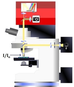
Figure 3. Optical diagram of a microspectrophotometer configured for incident illumination. Image Credit: CRAIC Technologies
Benefits of a Microspectrophotometer
MSP should be employed whenever it is not possible to determine the spectrum of a subpixel, defect, or micron-scale region of film using an instrument that only reports an area-averaged result.
MSP is primarily selected over other optical measurement approaches due to its combination of spatial resolution and full spectral fidelity. This combination is necessary due to three converging trends in display technology.
Shrinking Pixel Pitch
Current AR/VR, smartphone, and micro-display panels routinely exceed 400 to 1000+ pixels per inch, meaning that the space of individual subpixels is generally a few microns to a few tens of microns.
These individual subpixels cannot be resolved by a standard spectrophotometer with a typical minimum spot size of several millimeters. This instrument must integrate light from many pixels and any surrounding dark space, resulting in an aggregate and inaccurate spectrum.
Subpixel-Level Engineering
OLED emissive stacks are independently engineered for red, green, and blue emitters, each with distinct layer thicknesses, host-dopant chemistries, and microcavity designs.
Understanding and controlling these stacks requires spectral data that has been isolated to a single color's emitter as opposed to an average across the pixel group.
Defect and Non-Uniformity Analysis at Micron Scale
Dark spots, electrode shorts, particulate contamination, mura (visible non-uniformity), localized degradation, and other OLED failure modes manifest over areas smaller than traditional instruments’ spot size. Diagnosing these failure modes necessitates spatially resolved colorimetric or spectral data.
Research and Development Applications
Emitter and Material Characterization
Researchers use MSP during emissive-layer development to measure the electroluminescent spectrum of experimental host-dopant combinations deposited on patterned test pixels or small test substrates.
Test structures are regularly deposited as small, isolated pads to conserve costly novel materials. These pads may be just tens to hundreds of microns wide, meaning that an instrument capable of measuring these small areas is essential.
A full-panel spectroradiometer would require test structures that are much larger and more material-intensive.
Microcavity and Color-Tuning Studies
OLED stacks are regularly designed as optical microcavities to improve luminous efficiency and color purity. Cavity effects largely depend on layer thickness (down to the nanometer scale), meaning that R&D teams must assemble arrays of test pixels with deliberately varying layer thicknesses across a substrate.
MSP can be used to individually and rapidly measure each of these micron-to-millimeter-scale test sites, generating chromaticity and spectral data that can be used to build thickness-versus-color models.
Subpixel-Resolved Aging and Degradation Studies
Tracking the luminance decay and spectral shift of individual R, G, and B subpixels under accelerated aging conditions is beneficial to burn-in and lifetime studies.
Blue emitters generally degrade faster than red or green, meaning that it is necessary to isolate each subpixel's spectrum over time–as opposed to measuring a pixel group in aggregate–to build accurate degradation and compensation models suitable for use in subsequent panel firmware.
Viewing-Angle and Microcavity Off-Axis Behavior
Researchers can capture the shift in a single subpixel's spectrum with viewing angle by combining an MSP with a goniometric (angle-resolved) sample or detector positioning. This is a key input for compensating for angular color shift in sophisticated OLED architectures.
Color Filter and Optical Film Evaluation
MSP operated in transmittance/reflectance mode can be used to characterize the micron-scale transmission spectrum of individual color filter segments in white-OLED-plus-color-filter architectures, circular polarizers, and encapsulation stacks. This technique is used to confirm that filter design achieves the intended primaries.
Quality Control Applications
Subpixel Color-Point and Uniformity Verification
MSP-based systems (typically automated with motorized stages) sample subpixels on the production line or during incoming inspection to create spectral maps used to verify that emitted color coordinates fall within specification.
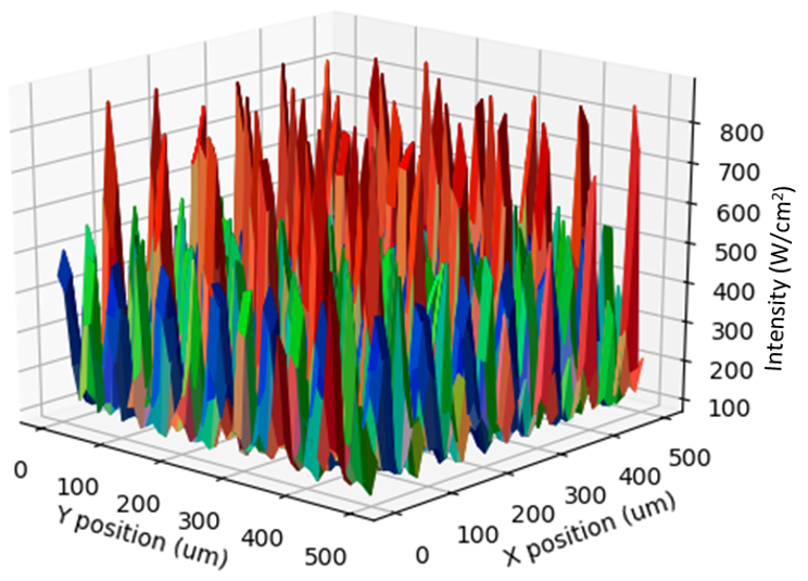
Figure 4. Luminance mapping of an advanced mobile phone display. Each hypercube of data contains a full spectrum at each point, which can be extracted (as shown in Figure 5). Image Credit: CRAIC Technologies
Mura and Defect Root-Cause Analysis
When a panel features mura or a localized defect, quality engineers employ MSP to obtain the anomalous region’s precise spectrum and luminance, comparing this to a known-good reference region at the same micron scale.
This allows them to determine whether the defect arises from a chromaticity shift, luminance shift, or both. This information also allows the failure to be traced to a specific process step, for example, particulate contamination, deposition non-uniformity, or electrode delamination.
Process Monitoring Across the Panel
Automated point-by-point MSP scans across a substrate can generate run-to-run and batch-to-batch spectral maps of film thickness, luminance, or chromaticity, which are used to monitor deposition uniformity (for example, shadow-mask drift or evaporation-source aging).
Incoming Material and Mask Inspection
Micron-scale reflectance or transmittance measurements can be used to confirm color filter registration, fine metal mask alignment marks, and encapsulation film optical properties prior to committing these to a full production run.
Advantages of Microspectrophotometry Over Alternative Techniques
Source: CRAIC Technologies
| Technique |
Limitation relative to MSP |
| Bulk spectroradiometer/colorimeter |
Large-scale sampling areas (often several millimeters) cannot isolate a single subpixel; the result is an area-averaged spectrum that masks subpixel-level defects and mixes red, green, and blue emission together. |
| Tristimulus (filter-based) colorimeter |
Measures only three or four broad color channels rather than a continuous spectrum, so it cannot detect subtle spectral shape changes (e.g., a shift in emission peak wavelength or a change in secondary emission peaks from a degrading dopant), and it lacks the spatial resolution that MSP provides. |
| Imaging colorimeter/2D color camera systems |
Provides good spatial coverage of luminance/chromaticity across a full panel but typically reconstructs color from limited (often three-channel, RGB-filtered) data rather than a true continuous spectrum, reducing accuracy for narrow or unusual emission features and for absolute colorimetric calibration. |
| Photoluminescence mapping without spectral dispersion |
Can map intensity spatially but, without a dispersive spectrometer, cannot report wavelength-resolved emission, so it cannot distinguish a luminance change from a color-shift change. |
| Electron microscopy/AFM |
Provides excellent spatial and structural resolution but no optical or spectral information; useful for structural defect analysis but not for verifying color and intensity performance. |
MSP is the only widely available technique able to simultaneously provide both micron-scale spatial selectivity and full, continuous spectral data with the accuracy required for rigorous colorimetric calculation, including correlated color temperature, CIE coordinates, and ΔE.
This combination empowers engineers to determine where an issue is located and to confirm what is spectrally different about it. Spot-integrating or channel-limited instruments simply cannot match these diagnostic capabilities.
Other practical advantages of MSP include:
- MSP is a non-destructive measurement, meaning that the same subpixel or test site can be re-measured after subsequent process steps or over time, for example, during aging studies.
- This single instrument is compatible with both reflective/transmissive and emissive modes, allowing a single tool to offer OLED emission characterization, thin-film inspection, and color filter evaluation capabilities.
- Motorized stages and software-driven measurement grids provide automation and repeatability, enabling the consistent sampling of large numbers of micron-scale sites. This is a key factor in academic reproducibility and effective statistical process control.
- Colorimetric output is calibrated and traceable, and spectral data can be converted directly into standard CIE color space values, supporting pass/fail QC criteria referenced to industry color standards and R&D characterization.
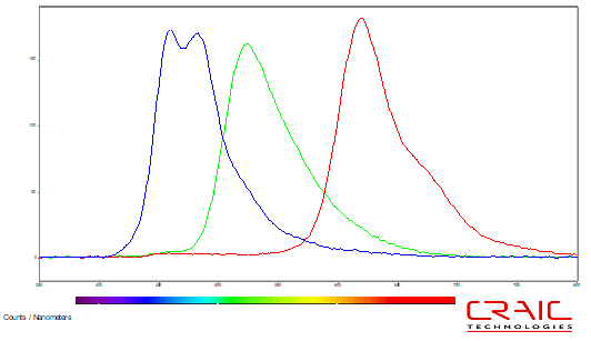
Figure 5. Spectrum of each colored pixel. This allows for rapid comparisons in both color and intensity of different pixels. Image Credit: CRAIC Technologies
Conclusion
Microspectrophotometers are increasingly indispensable in OLED display science, offering full spectral characterization at the same micron scale as the display's physical structure.
This capability makes them ideally suited to a range of R&D tasks, including microcavity tuning, emitter material development, and aging studies. Its applications in quality control range from mura root-cause analysis and subpixel color-point verification to production process monitoring.
Display pixel densities continue to increase, meaning that MSP’s spatial resolution advantage over simple colorimetric and bulk spectroradiometric techniques will continue to underpin OLED technology’s development and manufacturing quality assurance.

This information has been sourced, reviewed, and adapted from materials provided by CRAIC Technologies.
For more information on this source, please visit CRAIC Technologies.