A review of Ion Beam technology is presented in this paper. The key applications and benefits of using ion beam technology for etching processes in comparison to technology such as plasma etching will be presented.
An overview of ion beam generation is described, which will be followed by a discussion and presentation of some beneficial applications of ion beam technology.
Equipment and Technology
In essence, an ion beam source is a plasma source having a set of grids that enable extraction of a stream of ions. The three main parts of the ion beam source are the discharge chamber, the grids and the neutraliser.
Ion production is done in the discharge chamber by subjecting a gas like argon to an RF field. An alumina or quartz chamber having an RF-powered coil antenna around it intakes the fed gas. Free electrons are excited by the RF field until they have enough energy to break gas atoms into ions and electrons that can further ionize gas atoms ensuring that the gas is thus ionized and a plasma is established.
Capacitive coupling is suppressed in an OIPT ion source, by placing an electrostatic shield inside the quartz chamber to allow only the RF magnetic component to transfer energy to the gas atoms; hence ionization mainly takes place by an inductive coupling process. Furthermore to stopping the electrostatic shield stopping electric field, which is generated across the coil of the RF antenna, from entering the ion source, it also helps to break up any continuous conducting coating from depositing on the inside of the quartz plasma tube which could screen and reduce the plasma generation efficiency of the RF power.
The role of the grids is important for extraction and accelertion of ions to the required energy. The grid sets consist of two or three grids as shown in Figure 1a, which have a specific hole pattern with several apertures forming beamlets and a combination of all these individual beamlets form the broad ion beam. Grid curvature and inter-grid separation are also significant design features which depend on the application required, for example depending on the target size to be sputtered for deposition or substrate size and etch rate for etch applications.
The ion source generates a low temperature plasma with slow (cold) ions at an ion temperature less than 1eV, which can be extracted from the ion source through the grids with a well-defined energy.
In a three grid system, specific potentials or voltages applied between the grids provide the driving force and focussing optic for the ions. The inner grid in contact with the plasma, known as the “screen grid”, is the one that determines the beam voltage or energy. This is set at a positive potential relative to ground. The second “accelerator” grid is biased negative with respect to the ground, and offers the extraction voltage, which is the screen-accel potential difference for the beam ions. The third “decelerator” grid is normally grounded and helps beam collimation reducing divergence of the beam, minimises electron back-streaming and re-deposition of sputtered material back onto the accelerator grid. This in turn improves the period between down times for grid cleaning and also renders grids cleaning easier. The final energy of the accelerated ions is equal to the set beam energy or voltage (VB), as shown in Figure 1b.
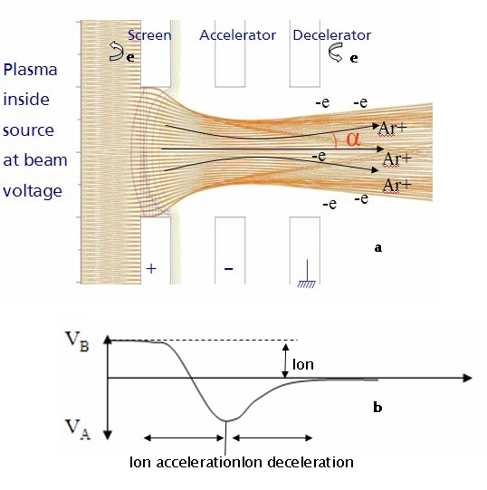
Figure 1. A three grid beam formation structure
Finally, the third element in the OIPT ion source is a neutraliser which is basically an electron source; the purpose of which is to balance the charge of the ions in the beam so as to reduce space-charge effects causing beam divergence through mutual repulsion of the ions and to prevent charging of the wafer or target surface. The basic Dual Ion Beam Sputtering (DIBS) chamber set up as comprises an etching source that precisely directs a neutralised ion beam onto a wafer located in the substrate holder. Normally, for good uniformity, the 15cm etch source can be used for wafers up to 4”, while the 30cm etch source is suitable for wafers up to 8”.
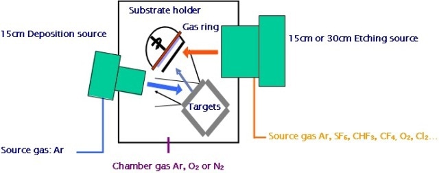
Figure 2. Schematic view of an Ionfab system
There are basically two types of etching: the first being Ion Beam Etching, or IBE, where only Ar, Xe, Ne or Kr (i.e. the noble inert gases) are used; this enables physical etching or sputtering and allows, among other processes, etching of noble metals and metal contacts auch as Au, Pt, Pd which are non-reactive materials and hence do not respond to reactive plasma or chemical etching as shown in Figure 3.
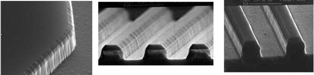
Figure 3. Left 0.3 µmCr etch, middle 3 µm Au etch, right 2 um deep Pt Ion Beam etch
Other suitable candidates are materials such as CMT that have some properties that need to remain unaltered after etching. IBE is preferred for etching stacks of multiple materials, such as MRAM devices, where a chemically-enhanced etch will be possible, but highly complex to optimise. This physical etching style is often termed ‘ion milling’.
The second type is Reactive Ion Beam Etching or RIBE where a chemically reactive gas such as SF6, CHF3, CF4, O2 or Cl2 (other gases can also be used) is usually added to Ar or other inert gas. There are two ways for introducing the reactive gas: either through the etching source or through the gas ring located on the substrate holder around the wafer. The gas ring mode is sometimes known as Chemically Assisted Ion Beam Etching or CAIBE.
Using chemically reactive gas, etch rates and selectivities to mask material can be improved. In RIBE mode, it is down to the combination of two processes that involve dissociation of the reactive species inside the ion source and the collision at the wafer surface between accelerated ions and reactive species. In CAIBE mode, only dissociation because of collision occurs, but it does have the benefit of controlling the inert and reactive gas partial pressures somewhat independently at the wafer surface.
Tilting of the substrate holder can be done between -90°, the loading position, and up to about +65°. The maximum angle depends on the chamber and endpoint options. In Figure 4, the platen is shown in loading position and at +45°. Indeed, tilt offers further control over the sidewall profile as well as radial uniformity optimisation. The substrate holder can rotate up to 20 rpm in order to provide an axisymmetric etch rate profile. The substrate and platen shaft are cooled by a dedicated chiller and helium is used as a conductive medium to transfer heat during etching.
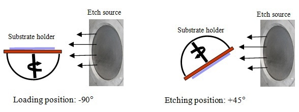
Figure 4. Schematic view of substrate holder positioning
A heating element imbedded within the platen enables the substrate to be heated to temperatures as high as 300°C. For example, etching InP with Cl2 is highly challenging when compared to etching GaAs with Cl2 and BCl3, since etch products containing In have poor volatility. Room temperature etching of InP with Cl2 results in a very rough surface due to remaining InCl2-based material on the surface. Increasing temperature above 150°C helps to increase etch rate by increasing volatility of products and enables a smoother surface to be obtained. With increasing temperature, the etching mechanism migrates from a more physical sputtering process to a more chemically oriented one (Figure 5).
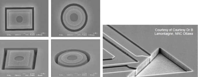
Figure 5. Left GaAs/AlGaAs etch with Cl2/BCl3, InP etch with Cl2 using platen heating.
Careful balance between the reactive gas, such as CHF3, and beam energy helps quartz to be etched at an angle as shown in Figure 6. CF4 reactive gas can also be used for deep anisotropic quartz etching.
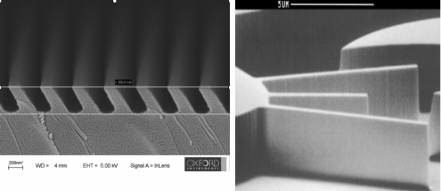
Figure 6. Left 300 nm blazed grating etch in quartz, 5 μm deep anisotropic quartz
Common artefacts with argon etching are spikes or ears, trenching, and rough surfaces. Trenching normally appears at the edges of the etch profile; these are because of a “double dose” effect of ions near the sidewall due to beam divergence and reflection from the walls. Ears or spikes are due to redeposition on the sidewalls after mask removal. Rough surfaces are usually caused during etching of polycrystalline substrates.
One solution for all of these problems is angled etch with rotation. The ‘double dose’ effect that causes trenching is evened out; sidewall deposition from the sides of the mask are resputtered off; the polycrystalline crystalites are effectively impacted by ions from all directions. The other significant factor is the mask (usually photoresist) profile. It is important to begin with a nice squared patterned resist in order to get nice vertical sidewalls after etching since argon etching (or milling) is a physical process that will effectively transfer the resist shape into the material to be etched. Selectivity between mask and etched material is usually around 1 (or even less) based on the material.
Determining the ideal parameters for a particular sample to be etched is based on the requirements, i.e. in terms of etch rate, side-wall shape and quality, maximum temperature that the mask can tolerate. For instance, depending on the parameters chosen, very good uniformity can be achieved over 200mm using the 30 cm etch source with a platen tilt of 10°, as can be seen in Figure 7. Here, the non-uniformity is below ±2% over ±95mm radius from wafer centre on a SiO2 coated Si wafer.
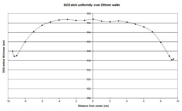
Figure 7. Example 1 of SiO2 etching uniformity over 200mm
In order to obtain the right parameters, where possible, the background work to determine etching parameters is done with SiO2 coated wafers. The recipe will usually transfer the uniformity in most cases. Certain applications may need a tighter uniformity over a smaller area, in which case different beam energy, gas flow, beam divergence and tilt angle might be required. Figure 8 shows this effect where uniformity across ±95mm radius is only about ±3.3% but in the region of ±65mm, uniformity is less than ±1% when platen tilt is set to 30° using different beam energy parameters.
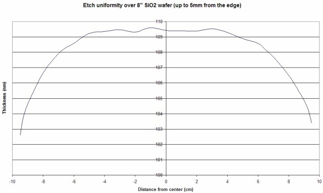
Figure 8. Example 2 of SiO2 etching uniformity over 200mm
These two examples here illustrate that a particular uniformity can be achieved, but not across the whole range of beam parameters and/or platen tilt angle. Again, etch uniformity is tightly linked with the sample geometry, the nature of the sample to be etched and the other process requirements. The curves in Figures 9 display the change in uniformity with tilt for one set of beam energy and gas flow values. In this particular case, the uniformity is optimized at a platen tilt of 10° (see Figure 4 for platen orientation). A general trend is that, with increasing tilt angle, non-uniformity reaches a point where it is minimum, then it will increase again as tilt angle is increased, see Figure 9 below.
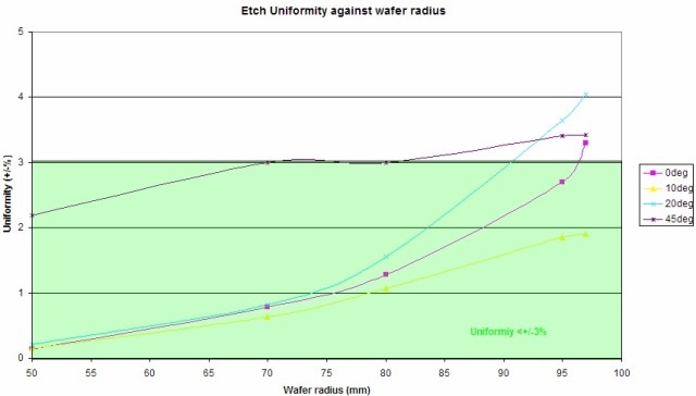
Figure 9. Example of SiO2 etching uniformity over 200mm with varying tilt angle
The end point detection (EPD) method typically employed in Ion Beam etching is second ion mass spectrometry or SIMS. In order to stop etching at a specific layer in multilayer structures of magnetic material or semiconductor devices, this option can be added to the tool capability. The impact of the primary ions at the surface of the sample being etched will generate secondary ions that have characteristics such as mass to charge ratio linked to the ions ejected from the sample. In Figure 10, the transitions between the various layers can easily be seen. When a layer is a compound, for example CoFe, Co is selected for monitoring as Fe is typically already present inside the chamber and components which would mask the sample signal.
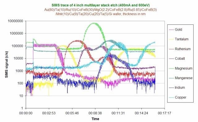
Figure 10. SIMS traces example of a multilayer stack
The platen rotation can be viewed clearly as small periodic variations on all signals. The SIMS signal is in counts per second and is monitored over time; thinner layers will normally use a slower etch rate to allow controllability of the SIMS end-point signal. In this example, the sample is 4” in diameter, but much smaller size samples down to as small as a 5 x 5 mm square can be still be monitored for end point.
It is possible to set up the SIMS probe based on the sample size, for the etch to allow maximum signal detection. Of course, the open area of material to be etched on the sample is also critical as the SIMS signal intensity is dependent on how much material is being etched and the incident beam current density.
Conclusion
Ion beam etching offers the following benefits:
- All materials can be etched including those that are not plasma etched
- Sidewall shaping is possible through sample tilting
- Etch rate can be improved by adding chemically reactive gases
- Independent ion beam current and energy control
- Excellent run for high repeatability
- Excellent uniformity
- Wide process versatility

This information has been sourced, reviewed and adapted from materials provided by Oxford Instruments Plasma Technology.
For more information on this source, please visit Oxford Instruments Plasma Technology.