Photonics is an emerging technology with a potential multitrillion euro market. Innovative small and medium sized enterprises (SMEs) are at the forefront of this development, but the R&D costs are prohibitive for them. That’s why 12 partners from northwestern Europe are creating an open access pilot line that will drastically reduce costs and time for the pilot production of new products. This new facility is projected to be the incubator of a thousand new companies and thousands of jobs. The 14 million euro project (OIP4NWE) is supported by the European Regional Development Fund and kicks off this week in Eindhoven.
 Representatives of the parties involved at the project kick-off meeting in Eindhoven this week.
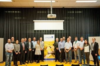
Photonics is much like electronics, but instead of electrons it uses light (photons) as its workhorse. It uses much less energy, it is faster, and it opens up a wealth of new opportunities. One of the key problems photonics will help tackle is the exploding energy consumption of data centers, as photonic microchips consume much less energy than their electronic predecessors. Another example is a high-precision monitoring system for aircraft wings, bridges or tall buildings.
After two decades of basic photonics research, the first companies producing photonic integrated circuits (PICs) are now taking off – sparsely. One of the main hurdles is the high cost involved in R&D. Not only does the PIC production require expensive high-tech equipment installed in cleanrooms, but currently the production processes still have a high defect rate and are too slow. This was workable for basic research but not for commercial R&D. The technology readiness level, which ranges from 1 to 9, needs to be jacked up from the current 4 to 7.
The new project, led by photonics stronghold Eindhoven University of Technology (in collaboration with its Photonic Integration Technology Center), consists of the realisation of an efficient pilot production line for shared use by European SMEs. It should take the defect rate in pilot production down and the throughput time will be shorter. All in all, this should lead to a cost reduction which significantly lowers the threshold for developing new photonic products. This should help establish a thousand integrated photonics firms within ten years after the project.
The front-end process (production of PICs on indium phosphide wafers) will be realised in the existing NanoLab@TU/e cleanroom facility at Eindhoven University. The PICs of different companies will be combined on one wafer to keep costs low. The back-end process is done at the Vrije Universiteit Brussel (optics for beam shaping and light coupling) and at Tyndall National Institute in Cork, Ireland (assembly of fiber-optic connections and electronics in the package). All steps require nanoscale precision to avoid product defects.
The first stage of the project is equipment installation. The second stage focusses on automation of the equipment while a third stage will involve intensive industrial research together with equipment manufacturers to optimize and develop new processes. The line should be fully in operation in 2022. To incentivize the initial uptake by SMEs, a voucher scheme for external SMEs will be set up.
The other parties involved are the companies AIXTRON SE (Germany), Oxford Instruments Nanotechnology Tools (United Kingdom), SMART Photonics, VTEC Lasers & Sensors, Technobis Fibre Technologies (all Netherlands) and mBryonics Limited (Ireland) along with research centers Photonics Bretagne (France), Cluster NanoMikroWerkstoffePhotonik.NRW (Germany) and Photon Delta Cooperatie (Netherlands).
The project has a total budget of 13.9 million euros. Of this, the EU is funding 8.3 million, with the remainder coming from the participating parties.