The PlasmaPro 100 Estrelas platform from Oxford Instruments has been developed to provide complete flexibility for Deep Reactive Ion Etching (DRIE) applications - serving a diverse set of process requirements across the Advanced Packaging, Micro Electromechanical Systems (MEMS), and Nanotechnology markets.
Specifically designed for research and volume production, the PlasmaPro 100 Estrelas provides the ultimate flexibility with Bosch and Cryogenic processes.
- High etch rate and high selectivity with the Bosch process
- Tapered through etches
- Higher mean time between cleans (MTBC)
- Enhanced reproducibility
- Highly anisotropic (vertical) profile
- Extensive range of applications
- Smooth sidewall and high aspect ratio processes
- Low rate and low power for nano-silicon etch and notch control (SOI)
- Electrostatic or mechanical clamping (substrates’ compatibility)
Video Credit: Oxford Instruments Plasma Technology
Overview
To obtain anisotropic profiles, the DSiE technique or the Deep Reactive Ion Etching (DRIE) repeatedly integrates isotropic silicon etching and passivation steps. With the help of a high-density plasma source and quick gas-switching capability, this method allows users to achieve smooth sidewalls, profile verticality, and high etching rates together with high selectivity to masking materials.
From high aspect ratio processes to tapered via etches and smooth sidewall processes to high rate cavity etches, the PlasmaPro 100 Estrelas has been creaed to ensure that the wide range of applications in MEMS, advanced packaging and nanotechnology can be realised without the need to change chamber hardware.
Nano and microstructures can be realized as the hardware has been designed with the capability to run Bosch™ and Cryo etch technologies in the same chamber.
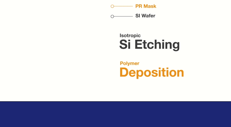
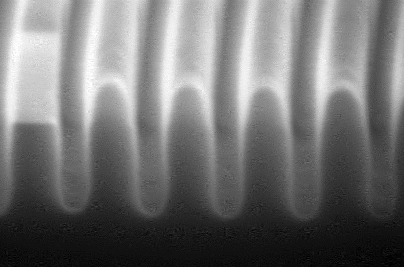
Bosch Process. Image Credit: Oxford Instruments Plasma Technology
Features
The platform is compatible with 50 mm to 200 mm substrates, guaranteeing that users have the chance to design devices that can be taken to production using the same chamber hardware.
- Auto match — Process flexibility
- Fast-acting close-coupled MFCs — Quick control (originally developed for ALD)
- Higher flow MFCs and associated generators — High radical densities
- Reduced chamber volume and high throughput pumping — Guarantees high gas conductance
System Requirements
- High-density plasma (chemically driven process)
- Sophisticated recipe editor
- Close-coupled gas pod
- Effective wafer cooling
- High flow and pumping
- Rapid and simple switching from liquid nitrogen (LN2) to the chiller and vice-versa
- Heated liners and top plate
Applications
Bosch Applications
Normally, Bosch DSiE is utilized for features >1 µm and depths >10 µm, including:
- MEMS for Smart Devices, Consumer, and Industrial Electronics
- Microfluids
- Through Silicon Via (TSV)
- Biomedical devices
- SiO2 and Quartz Etch
- High Q Capacitor Arrays and High Q Resonators for Quantum Devices
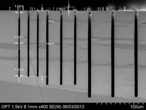
Image Credit: Oxford Instruments Plasma Technology.
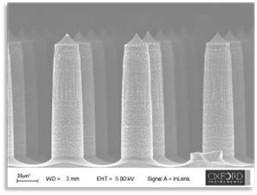
Image Credit: Oxford Instruments Plasma Technology
Cryogenic Applications
Normally, cryogenic DSiE is utilized for smooth sidewalls and/or nano-etching and temperature-sensitive materials, as it offers a low-temperature process (−110 °C).
- Photonics
- Nano applications
- Molding
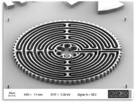
Image Credit: Oxford Instruments Plasma Technology
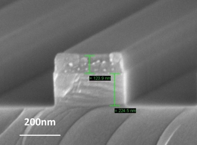
Image Credit: Oxford Instruments Plasma Technology
Specifications
Table 1. Source: Oxford Instruments Plasma Technology
| Parameter |
Bosch |
Cryogenic |
Mixed Gas |
| Rate (?m/minute) |
High |
Moderate |
Low |
| Selectivity to PR |
Very High |
High |
Low |
| Profile |
Vertical |
Vertical or Sloped |
Vertical or Sloped |
| Aspect Ratio |
Very High |
High |
Low |
| Sidewalls |
Scallops |
Smooth |
Smooth |
| ARDE control |
Yes |
Limited |
Limited |
| Cleaning |
Regular |
Rare |
Regular |
| Min. feature /nm |
≈ 300 |
≈ 10 |
30 |
Atomic Layer Etching (ALE)
Atomic Layer Etching (or ALE) is a sophisticated etch method enabling outstanding depth control on shallow features. As device feature size decreases, ALE is required to achieve the accuracy needed for peak performance.
High-fidelity pattern transfer (etching) is necessary for the fabrication of present advanced microelectronic devices. Since features reduce to sub-10 nm levels and novel devices utilize ultra-thin 2D materials, there is a growing need for atomic-scale fidelity.
This has resulted in an increasing interest in a method called Atomic Layer Etching (ALE), which circumvents the limitations of traditional (continuous) etching at the atomic scale. Plasma-based atomic layer etching is a cyclical etching process of gas dosing and ion bombardment that eliminates material layer by layer and has the potential to eliminate single atomic layers with very low damage.
How Does Atomic Layer Etching Work?
Video Credit: Oxford Instruments Plasma Technology
Process Benefits
- Achieves etching of layers with high-depth precision
- Low damage to underlying substrates
- Up to 200 mm wafer with normal uniformity <±2%
- Can be utilized together with standard ICP
- Advanced technology for high control of etch depth
Atomic Layer Etching Process
Normally, Atomic Layer Etching includes a cycle of four steps that are repeated as required to obtain the necessary etch depth. The example below highlights ALE of AlGaN etching with Cl2/Ar.
Step 1) Dosing of the substrate with an etching gas, which adsorbs on and reacts with the etch material. The etch gas is frequently plasma separated to improve the rate of adsorption. With the proper choice of dosing gas and parameters, it could be self-limiting if the chemical dose stops following adsorbing one monolayer.
Step 2) Purging of all residual dose gas.
Step 3) Bombardment of the surface exhibiting low energy inert ions, which eliminate the reacted surface layer. This could be self-limiting if the energy of the ions is enough to eliminate the chemically modified layer but inadequate to (sputter) etch the basic bulk material.
Step 4) Etching products are purified from the chamber.
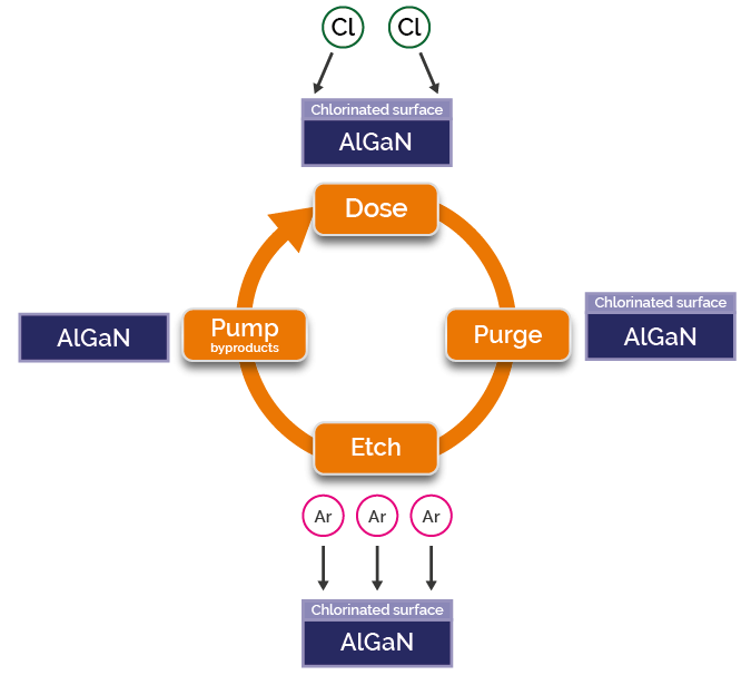
Image Credit: Oxford Instruments Plasma Technology
Key Benefits
Benefits of Atomic Layer Etching
- Low damage etching, as a result of the use of low ion energies
- Self-limiting behavior
- Accurate control of etching depth
- High selectivity, as dose gas and ion energy can be customized to reduce the etching of mask layers or basic materials
- Ultra-thin layer removal
- Smooth etch surfaces
- Anisotropic in nature, as a result of the reliance on ion bombardment
- Etch rate is least impacted by the aspect ratio of etched features (that is, reduced ARDE), as the supply of radicals and surface ion bombardment have been isolated into separate steps
- Enhanced uniformity, as a result of its self-limiting nature
Image Credit: Oxford Instruments Plasma Technology
ALE Features
- Etch rates 2 to 7 Å/cycle
- Rapid recipe control down to 10 milliseconds
- Illustrated outcomes in a-Si, Si, MoS2, SiO2, GaN, AlGaN layer etching
- Atomic Layer Deposition-style gas dose delivery happens with 10-millisecond open-close response
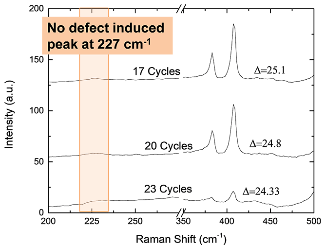
ALE of MoS2 shows no Raman defect peak after etching, highlighting the low damage etching capabilities of ALE. Image Credit: Oxford Instruments Plasma Technology
25 nm wide Si trenches etched to 110 nm depth by ALE, HSQ mask still in place. Image Credit: Oxford Instruments Plasma Technology
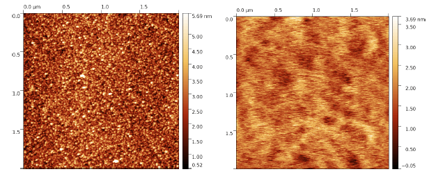
AlGaN surface roughness after 200 ALE cycles, left = before etching (Ra = 600pm), right = after etching (Ra = 300pm). The surface has been smoothed by ALE. Image Credit: Oxford Instruments Plasma Technology
ALE Processes
Wide Range of Materials
ALE is ideal for an extensive range of materials, such as Si, a-Si, SiO2, MoS2, GaN, AlGaN, III-V’s, Si3N4, graphene, HfO2, Al2O3, ZrO2, metals, etc.
Table 2. Source: Oxford Instruments Plasma Technology
| Material Etched |
Dose Gas |
Etch Gas |
| MoS2 |
Cl2 |
Ar |
| Si or a-Si |
Cl2 |
Ar |
| SiO2 |
CHF3 or C4F8 |
Ar or O2 |
| AlGaN or GaN |
Cl2, BCl3 |
Ar |
| AlGaN or GaN |
N2O |
BCl3 |
| GaAs or AlGaAs |
Cl2, BCl3 |
Ar |
| InP or InGaAsP etc. |
CH4, Cl2 |
Ar |
| SiN |
H2 |
Ar |
| Al2O3 |
BCl3 |
Ar |
| Graphene |
O2 |
Ar |
| HfO2, ZrO2 |
Cl2, BCl3 |
Ar |
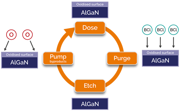
AlGaN ALE Process Cycle. Image Credit: Oxford Instruments Plasma Technology
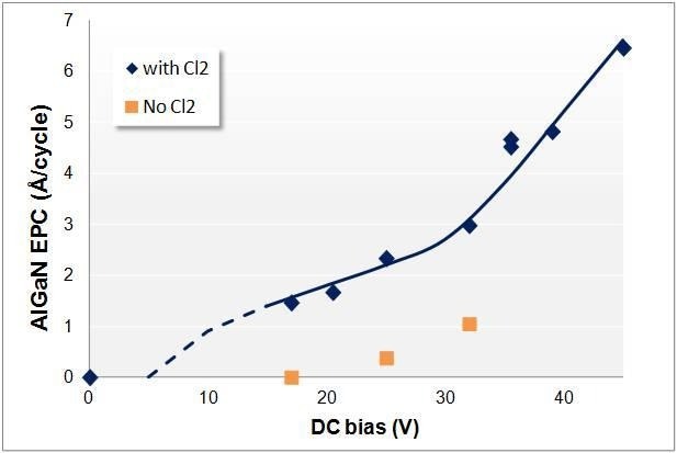
AlGaN Etch per Cycle with and without Chlorine dose. Image Credit: Oxford Instruments Plasma Technology
PlasmaPro 100 ALE
The Atomic Layer Etching equipment is constructed based on 13+ years of experience.
Listed below are the key features:
- Quick recipe control, down to 10 milliseconds
- Dose gas pulses down to 10 milliseconds, providing outstanding control of dose quantity
- Integrated traditional and atomic layer etching can be done in a single tool, with mode selection through software recipe control
- Chamber and source design proven for ALE and standard etching
- Outstanding control of ion energy, along with power control down to 0.3 W in increments of 0.1 W
- Patented hardware (US 10,008,369 B2)
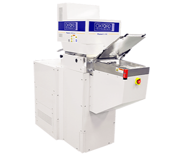
Image Credit: Oxford Instruments Plasma Technology