As advances in semiconductor devices demand tighter tolerances, smaller interconnects, and more vertical layers, product quality and reliability need to be ensured by quickly, accurately, and non-destructively identifying latent defects early in the manufacturing process.
The X200 from Bruker integrates high speed and high resolution to provide a one-of-a-kind, no-compromises, in-line X-Ray defect inspection solution. To provide fully automatic, fast, 100% inspection, and real-time feedback, X200 employs proprietary data collection architecture, industry-leading data processing, and innovative machine learning techniques.
Only the X200 Delivers
- Rapid, high-resolution X-Ray imaging that finds even the smallest latent defects across an entire die in seconds
- Complete automation from imaging to data processing, with real-time feedback for constant use on the manufacturing floor
- Advanced Data Analysis Toolkit with image processing-based machine learning algorithms to accelerate and standardize defect detection
Incorporating metrology process feedback into the manufacturing process is essential to:
- Attaining a defect rate <100 ppb
- Lowering excursion discovery time from weeks to days
- Increasing learning during prototype ramp
- Decreasing time to high-volume manufacturing (HVM)
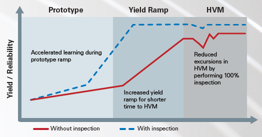
Image Credit: Bruker Nano Surfaces and Metrology
Redefining X-Ray Defect Inspection
As X-Rays penetrate deeper into materials than light or electrons, they are an effective method for detecting defects that are not visible on the surface of a substrate. There are various types of X-Ray imaing (XRI), but the most common uses attenuation contrast to exploit material differences in X-Ray absorption coefficients.
Bruker has optimized X-Ray imaging with the X200 to make full defect inspection possible in-line on the manufacturing floor. Instead of pulling a small sample from the line for time-consuming and data-limited 3D X-Ray and cross-sectioning, 100% of production can be automatically monitored in real time for maximum quality, reliability, and yield.
Resolving Process Versus Defect
Defect detection does not require resolving each defect for visualization. The X200 continuously measures bump quality, which can be used for pass-fail qualification as well as binning for device performance and reliability.
Defect Screening
- Use sensitive metrics to identify latent defects like solder necking, head-in-pillow, non-wet cracks, and other marginal bumps
- Flag bump defects, including bridges, non-wets, and voids
- Generate an automatic defect classification model for identifying failure modes quickly
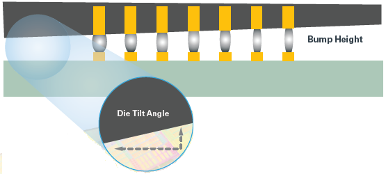
Die tilt affecting bump height and causing non-wet defects. Image Credit: Bruker Nano Surfaces and Metrology.
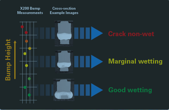
The X200 can measure bump height, a predictive indicator of wetting behavior. This requires no cross-sectional or high-resolution defect imaging beyond initial validation step. Image Credit: Bruker Nano Surfaces and Metrology.
Die-Attach Process Control
- To evaluate the quality of the die-attach process, evaluate each bump shape across the entire device
- Provide corrective feedback to die-attach tools on process parameters, including die shift, rotation, height, tilt, and warpage
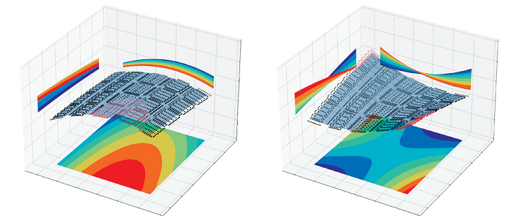
Die warpage can be intuitively represented in 3D by mapping bump heights, which can also be used to flag non-wet defects. Image Credit: Bruker Nano Surfaces and Metrology.
X200 Specifications
Source: Bruker Nano Surfaces and Metrology
| Physical Parameters |
Operating Parameters |
Facilities Requirements |
Tool Dimensions (WxLxH):
2.06 m x 2.85 m x 2.19 m |
X-ray Source: Tungsten target, 1000 W, 14 mA, 70 kV |
Electrical: 208 V AC (3-phase)/5-wire/8 AWG |
| Load Height: 0.957 m above floor |
Detector: 30 MP, 16-bit, 18 mm x 12 mm FOV @ 2.8 μm pixel |
AC Frequency: 50–60 Hz |
| Tool Weight: 6,300 kg |
Substrates: 200/300 mm wafers, film frame, strips (with/without boat cassette carrier), singulated parts |
AC Current: 22/40 A (load/main circuit breaker) |
| Cleanroom FFU: ULPA filters @ 0.12 μm |
Substrate Size (Max): 380 mm x 380 mm, thickness <5 mm |
CDA: 90–140 PSIG (filtered 0.25 μm, 5 CFM minimum, 10 mm tube) |
| Compliance: S2, S8, S14, and NFPA79 |
Substrate Bow/Warp: <3 mm center-to-edge |
Vacuum: 18–22 in-Hg (1 CFM, 10 mm tube) |
| Tool Frame: Steel |
Substrate Weight (Max): <2.2 kg |
Heat Exhaust: 8 in exhaust (2 pl), 2000 CFM total |
| X-ray Shielding: All exterior surfaces, FDA approved |
Substrate Load Modules (sold separately): EFEM, strip handler |
Ambient Humidity: 8-90% (non-condensing) |
| Safety Interlocks: All hinged doors are electronically locked, interlocked switches, EMO |
Automation: SECS/GEM, GEM300 |
Ambient Operating Temperature: 55–88 °F |