A new benchmark has been set by the ContourX-100 Optical Profilometer for precise and repeatable non-contact surface metrology at a best-in-class price point.
The compact footprint system provides uncompromised 2D/3D high-resolution measurement abilities in a simplified package that integrates several years of proprietary Bruker white light interferometry (WLI) innovation.
Next-generation improvements include a new 5 MP camera and updated stage for bigger stitching abilities, and a new measurement mode, USI, for even bigger convenience and flexibility for accuracy in thick films, machined surfaces, and tribology applications. Users will not be able to find a benchtop system with improved value compared to the ContourX-100.
Industry-best Z Resolution
Provides constant, precision measurements, independent of magnification.
User-Friendly Software Interface
Offers intuitive access to a wide library of pre-programmed filters and analyses.
Unmatched Metrology Value
Offers a simplified design without compromised measurement abilities.
Features
Unparalleled Metrology
The ContourX-100 profiler is known to be the culmination of more than 40 years of proprietary optical innovation and industry leadership in non-contact surface metrology, characterization, and imaging.
The system makes use of 3D WLI and 2D imaging technology for several analyses in an independent acquisition. ContourX-100 is strong in all surface situations ranging from 0.05% to 100% reflectivity.
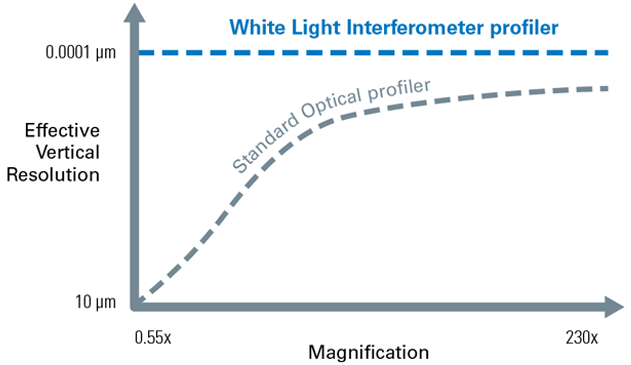
WLI offers constant and ultimate vertical resolution for all objectives. Image Credit: Bruker Life Sciences Mass Spectrometry
Unmatched Value and Analysis
With the availability of thousands of tailored analyses and Bruker’s simple and strong VisionXpress™ and Vision64® user interfaces, the ContourX-100 benchtop has been improved for productivity in both laboratories and on factory floors.
The hardware and software tend to integrate to offer simplified access to top high-throughput optical performance, thereby entirely excelling comparable metrology technologies.
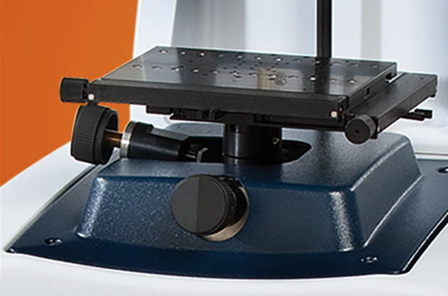
ContourX-100 manual stage. Image Credit: Bruker Life Sciences Mass Spectrometry
Applications
Surface-Independent Metrology with Application-Specific Solutions
Precision Engineering
Users can hold the surface texture and geometric dimensions of precision-engineered parts within the strict specification limits. The gage-capable measurement systems offer effective feedback and reporting as users tend to monitor, track, and calculate processes and assess GD&T conformance.
Image Credit: Bruker Life Sciences Mass Spectrometry
MEMS and Sensors
High-throughput and highly repeatable etch depth, film thickness, step height, and surface roughness measurements can be performed by the users, as well as sophisticated critical dimension metrology of MEMS and optical MEMS.
Optical profiling has the potential to characterize devices across the manufacturing process from wafer to final test, and even via transparent packaging.
Image Credit: Bruker Life Sciences Mass Spectrometry
Orthopedics/Ophthalmics
Users can achieve accurate, repeatable measurements of implant materials and components via the complete product life cycle. The WLI optical profilers aid QA, R&D, and QC analyses.
This can be done for applications varying from the characterization of surface parameters of lens and injection molds to surface finish verification and wear of medical equipment.
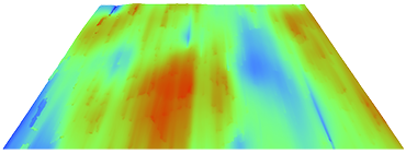
Image Credit: Bruker Life Sciences Mass Spectrometry
Tribology
It is possible for users to quantify, analyze, and regulate the effect of wear, friction, lubrication, and corrosion on material or component performance and lifespans. They can also identify quantitative wear parameters and execute fast pass or fail inspections on the extensive range of smooth, shiny, or rough surfaces.
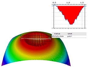
Image Credit: Bruker Life Sciences Mass Spectrometry
Semiconductors
Users can improve productivity and decrease costs for both front- and back-end manufacturing processes with the help of automated, non-contact, wafer-scale metrology systems.
Execute post-CMP die flatness inspection; coplanarity, bump height, and defect identification and analysis; and quantify the vital dimensions of component structures.
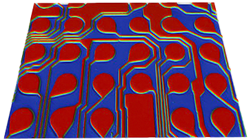
Image Credit: Bruker Life Sciences Mass Spectrometry
Optics
Users can gain better insights into the root causes of defects and improve polishing and finishing processes with precise and repeatable sub-nm roughness measurements.
The non-contact metrology systems allow compliance with growing stringent specifications and ISO norms for samples varying from small aspheric and free-form optics, to optical components with complicated geometries, to diffraction gratings and microlenses.
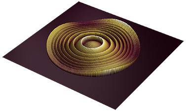
Image Credit: Bruker Life Sciences Mass Spectrometry