Jul 2 2009
The wafer-processing section at this year's SEMICON West will feature engineers from CyberOptics Semiconductor discussing the role of a newly developed particle-sensing technology to monitor airborne particles in process equipment in real-time to validate and analyze wafer contamination.
 CyberOptics Semiconductor developed the new WaferSense(R) Airborne Particle Sensor (APS) to allow engineers to efficiently detect and classify particles and their exact sources in a process as wafers are transferred, slit valves actuate and chambers are cycled, pumped down and purged. The APS is compatible with front-ends, coater/developer tracks, deposition and etch equipment.
The company developed the new wireless particle-sensing technology during the last year and demonstrated prototypes of its new WaferSense® Airborne Particle Sensor (APS) in fabs and OEMs -- in preparation for the launch at SEMICON West, according to Craig C. Ramsey, Ph.D., CyberOptics Semiconductor's general manager and CTO.
Ramsey said the new APS will be ready for purchase-order fulfillment in 2H09, and the wafer-like device is designed to "lower the time and expense of process equipment particle qualification, as well as raise die yields."
CyberOptics Semiconductor will demonstrate the APS and its entire line of WaferSense metrology devices at booth 5761 in the North Hall at SEMICON West.
"When process engineers have real-time views of particle conditions and can address specific trouble spots -- rather than guess-and-check throughout the whole tool -- they're far better prepared to pass particle qualifications on the very first attempt," Ramsey said. "When a tool fails particle qualification, APS can be used to discover where in the process particles were added to monitor wafers."
Ramsey observed that fabs which are unable to isolate and mitigate the source of particles in a tool before wafer processing experience reduced die yield due to wafer contamination.
CyberOptics Semiconductor developed the APS to allow engineers to efficiently detect and classify particles and their exact sources in a process as wafers are transferred, slit valves actuate and chambers are cycled, pumped down and purged, according to Ramsey. APS is compatible with front-ends, coater/developer tracks, deposition and etch equipment.
The APS is designed to help fabs "reduce their overall cost of operation by reducing equipment downtime, monitor wafer consumption and engineering labor," Ramsey said. Fabs gain additional efficiencies from the reduced surface particle metrology equipment loading and run more smoothly when their metrology queues remain short.
Ramsey added that the automation-friendly, vacuum-compatible device doesn't require engineers to open chambers or expose ultra-clean process areas to atmospheric gases. Testing has shown the sensor has the ability to detect 0.1 um particles. The self-contained device uses a fan to pull particle-contaminated gas through a channel as a laser illuminates the gas stream while particles scatter light on to the sensor's photo-diode detectors.
Fab engineers validate and analyze the particle conditions in process equipment with the device's companion software, ParticleView™ and ParticleReview™. ParticleView's GUI displays cumulative or differential particle counts and allows users to mark log files to indicate where, exactly, the device is in a process for real-time partitioning. ParticleReview's GUI displays log-file data obtained by the APS to allow users to conduct machine-to-machine trend analysis of particle conditions and to establish process control and conduct process improvement.
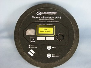
The WaferSense APS' specifications and features include form factors of 200 and 300 mm, with 450 mm versions to be available by special order. The APS, like other WaferSense devices, uses a wireless Bluetooth link and is compatible with Windows 2000, XP and Vista.
The WaferSense APS package includes the particle-sensing wafer, USB-compatible link, ParticleView and ParticleReview software, charging clean box and suitcase.
The WaferSense family of devices includes the Auto Vibration System (AVS), Auto Leveling System (ALS2 Vertical), Auto Teaching System (ATS) and Auto Gapping System (AGS). Each device follows the processing life of a wafer and reports real-time metrology data.