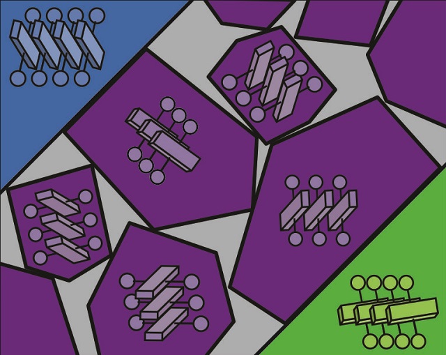
 Sketch of organic semiconductor thin film shows that the interfacial region between larger domains (blue and green) consists of randomly oriented small, nano-crystalline domains (purple).
Organic semiconductors can be easily printed using solution, making them as an inexpensive, scalable substitute to silicon-based devices. They are employed in photovoltaic cells, field effect transistors, and LEDs.
However, a major drawback of these semiconductors is their inconsistent performance originating in the domain interfaces of the organic semiconductor thin films. The root cause of the problem was unclear until now. The issue has now appeared to have been solved with the use of an innovative microscopy technique by Berkeley Lab researchers.
The new microscopy is capable of analyzing the domain interfaces in TIPS-pentacene, a high-performing solution-processed organic semiconductor. The research team has identified that randomly organized nanocrystallites have been kinetically trapped in the domain interfaces in the process of solution casting. These nanocrystallites tend to hinder the flow of charge-carriers.
If the interfaces were neat and clean, they wouldn’t have such a large impact on performance, but the presence of the nanocrystallites reduces charge-carrier mobility. Our nanocrystallite model for the interface, which is consistent with observations, provides critical information that can be used to correlate solution-processing methods to optimal device performances.
Naomi Ginsberg, a faculty chemist with the U.S. Department of Energy (DOE)’s Lawrence Berkeley National Laboratory and the University of California (UC) Berkeley
The study published in the Nature Communications journal was led by Ginsberg, who holds appointments with UC Berkeley’s departments of chemistry and physics, and Physical Biosciences and Materials Sciences Division of Berkeley Lab. The co-authors of the paper titled "Exciton dynamics reveals aggregates with intermolecular order at hidden interfaces in solution-cast organic semiconducting films" are Hao Wu, Benjamin Cotts and Cathy Wong.
The ability of carbon to create large molecules like pentacene and benzene forms the basis of organic semiconductors. These molecules exhibit electrical conductivity between insulators and metals. Without the need of costly high-temperature annealing used in silicon and other inorganic semiconductors, organic materials are easily fabricated in the form of crystalline films through solution-processing. Although it has been revealed that the performance of organic devices is based on the crystalline domain interfaces, comprehensive details on the morphology of domain interfaces still remain unknown.
Interface domains in organic semiconductor thin films are smaller than the diffraction limit, hidden from surface probe techniques such as atomic force microscopy, and their nanoscale heterogeneity is not typically resolved using X-ray methods. Furthermore, the crystalline TIPS-pentacene we studied has virtually zero emission, which means it can’t be studied with photoluminescence microscopy.
Naomi Ginsberg
The team used transient absorption (TA) microscopy to overcome the challenges. In TA microscopy, the transient energy states are excited by femtosecond laser pulses and the corresponding variations in the absorption spectra are measured using detectors. The researchers applied TA microscopy on their own optical microscope to produce focal volumes that are smaller than traditional TA microscopes by thousand times. They also used multiple different light polarizations to isolate interface signals that are not visible in the adjacent domains.
Instrumentation, including very good detectors, the painstaking collection of data to ensure good signal-to-noise ratios, and the way we crafted the experiment and analysis were all critical to our success. Our spatial resolution and light polarization sensitivity were also essential to be able to unequivocally see a signature of the interface that was not swamped by the bulk, which contributes much more to the raw signal by volume.
Naomi Ginsberg
This novel technique that unveils the structural patterns present in the hidden interfaces of the organic semiconductor thin films should provide a predictive factor to ensure cost-effective and scalable solution-processing of organic materials. It should also aid mitigating discontinuities and optimizing the movement of charge carriers. At present, researchers employ a trial-and-error method, which involves testing different solution casting conditions to assess the performance of resulting devices.
Our methodology provides an important intermediary in the feedback loop of device optimization by characterizing the microscopic details of the films that go into the devices, and by inferring how the solution casting could have created the structures at the interfaces. As a result, we can suggest how to alter the delicate balance of solution casting parameters to make more functional films.
Naomi Ginsberg
References