DSM 982, the first field emission scanning electron microscope with Gemini technology, was introduced in 1993. The resolution of the system was 3 to 4 nm at 1 kV, which set a new standard for low voltage SEM (LVSEM) and dramatically extended the field of field emission scanning electron microscopy (FE-SEM) applications into low landing energies. Some of its major benefits include increased SE yield, reduced sample damage, and higher surface sensitivity for higher resolution, due to a small beam and smaller interaction volumes.
The Gemini optical column integrates the beam booster and the Gemini objective lens. The latter is a compound magnetic-electrostatic objective lens, as shown in Figure 1. When such a lens is used, the spherical and chromatic imaging aberrations decrease considerably with decreasing beam energy.
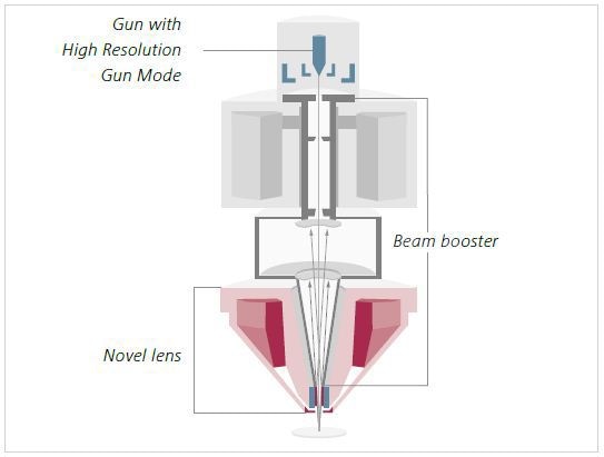
Figure 1. Schematic cross-section of Gemini optical column with new high resolution gun mode, beam booster, Inlens detectors, novel lens design (compound lens consisting of magnetic and electrostatic lens).
The Gemini column features a new optical design with a sophisticated lens design and gun mode. The Gemini objective lens has been further improved by optimizing geometry, and magnetic and electrostatic field distributions.
It now gives 1.2 nm at 500 V. Moreover, usability issues like additional fields at the sample are also eliminated. A unique gun mode was also designed so as to reduce the energy spread of the main beam. The effect of the chromatic aberration is further reduced to facilitate even smaller probe sizes, and maintain an adequate resolution even at less than 1 kV.
The performance of the electron optic system is improved, and at the same time, field effects at the sample are reduced as much possible. The Gemini objective lens provides superior imaging conditions even on complex samples.
The Gemini beam booster technology not only ensures small probe sizes, but also promotes high signal-to-noise ratios down to low accelerating voltages. The sensitivity of the system to external stray fields is reduced by maintaining the beam at a high voltage all through the column until its last deceleration.
Gemini Technology Enables High Resolution at Low Voltage
In order to prevent beam damage, and to balance the beam current and SE yield for charge neutrality, high resolution at low voltage is required. Using the following application examples (Figures 2A and B), it was possible to obtain exceptional imaging conditions in beam sensitive, charging materials like FeO(OH) or in charging samples like Al2O3.

Figure 2. a) Nanometer spaced FeO(OH) crystals at imaged at 1 kV. Sample: courtesy of L. Maniguet, INP Grenoble, FR.

Figure 2. b) Surface of a Al2O3 sphere.

Figure 2. c) Etched silicon nano-structures imaged at 50 V beam voltagewithout sample biasing. Sample: courtesy of A. Charai, Aix Marseille University, France.

Figure 2. d) Mesoporous Silica imaged at 500 V.
Detection Technology - Detectors for High Resolution, Sensitivity and Efficiency
Through the Gemini detection concept, efficient signal detection is realized by detecting backscattered (BSE) and secondary (SE) electrons in parallel. The Inlens detectors, assembled on the optical axis, reduce the necessity for realignment, and hence reduces time to image.
The optimization of detection efficiency and high resolution properties offers high quality SEM images. In addition, the Gemini objective lens, featuring a new design, improves in-lens SE detection because it functions as an imaging lens, and also improves detection for BSE and SE electrons produced by the sample. Here, the in-lens SE signal is 20x higher than that of traditional SEM designs. This allows imaging at low voltages with rapid scan speeds for high speed sample analysis.
Figures 2C and D show the flexibility of using different voltages. Voltages of 500 V or even 50 V can be used to obtain images having a good signal-to-noise ratio. In zeolite, it was possible to image channels down to sizes of a few nanometers (Figure 2D).
In this case, the integration of good detection efficiency and high resolution is important and can be realized without biasing the sample holder. Furthermore, the energy filtering characteristics of the Gemini lens are useful for imaging doping profiles of semiconductor structures with improved voltage contrast.
Detection Technology - Inlens EsB Detector for Energy Filtering and Detection of Low Voltage BSE
The Inlens EsB (energy selective backscatter) detector is a second detector on the optical axis in the column. With an energy filtering grid, this detector allows a separation of BSE and SE electrons. Energy filtering can be utilized to improve the contrast of material for low loss BSE owing to spectral variations. This latest trend of searching for spectroscopic data of the detected electrons is now increasingly being used.

Figure 3. a) Catalyst: Silver nano-particles embedded in Zeolite, SE (left) and EsB (right), at 1.5 kV. Sample: courtesy of G. Weinberg, Fritz-Haber-Institute of the Max-Planck society, Germany.

Figure 3. b) BaFe12O19 nano-particles shows 1.1 nm (002) lattice spacing. Sample: courtesy of H. Romanus, TU Ilmenau, Germany.

Figure 3. c) Lithium ion battery cathode material, BSE compositional contrast, no damage in sensitive binder material. Sample: courtesy of T. Bernthaler, Materials Research Institute Aalen, Germany.

Figure 3. c) Gold on carbon sample, BSE channeling contrast.
Detection Technology - STEM and BSE
Besides the in-lens detectors, enhanced semiconductor detectors are also available for scanning transmission electron microscopy (STEM) and BSE imaging. Both these are provided as semiconductor multi-segment detectors. The common aspects of these retractable detectors are excellent signal-to-noise ratios, and angular sensitivity at relatively low voltages.
It is possible to read out the segments separately, in various combinations, and up to four signals in parallel. For the BSE detector, the standard modes include topographical or compositional imaging with the BSE electrons. For the STEM detectors, this allows the commonly used Oriented darkfield (ODF), brightfield (BF), and High angular annular darkfield (HAADF) modes.
The Bariumhexaferrites are magnetic nano-particles which have multiferroic properties. Here, it is possible to obtain lattice resolution in the Gemini SEM, determined in transmission with the STEM detector (Figure 3B). It is also possible to obtain channeling and compositional BSE contrasts by semiconductor multi-segment backscatter detectors.
For lithium battery analysis, users can locate binder material adjacent to the lithium cobaltate. The microstructure visibly shows the deterioration of a lithium battery (Figure 3C). For easy backscatter imaging at higher pressures, this detector is incorporated into an aperture can be utilized in low vacuum, with different pressure variations.
Variable Pressure Technology
The advanced variable pressure (VP) technology provides enhanced signal detection efficiency and allows operation at higher pressures with high resolution. This enables the highest flexibility utilizing all detectors from high vacuum, such as VPSE, SE, Inlens EsB, Inlens SE, and BSD detectors.
Overview of Variable Pressure
In the variable pressure scanning electron microscopy (VPSEM), the inelastic scattering of BSE electrons and beam with gas atoms generates positive ions and free electrons. The charged species are attracted to the charged regions on the surface of the sample and are discharged.
This gas ionization procedure is further increased by SE and BSE electrons produced from the specimen. These electrons are consequently accelerated by the VPSE detector and the applied potential of the pressure-limiting aperture (PLA). The new VP technology not only reduces the skirt effect in high gas pressure, but also allows detection of the SE signal using Inlens detectors.
Pressure-Limiting Aperture
The main component of the newly developed VP technology is a retractable pressure-limiting aperture, as shown in Figure 5. When in place, this aperture allows up to 500 Pa pressure in the specimen chamber, whilst the pressure in the objective lens is kept in high vacuum. The beam booster can be used during VP operation so that high resolution can be achieved at low beam energy. Table 1 shows the excellent flexibility of the VP system. Figure 4 illustrates the enhancement of the new VPSE in comparison to traditional VPSE technology.
Table 1. Vacuum modes for the new VP concept
| Mode |
pressure-limiting aperture |
Booster |
Chamber Pressure (Pa) |
| High Vacuum HV |
None |
On |
< 10-2 |
| Variable Pressure VP |
None |
Off |
5 – 30 |
| Nano VP |
800 µm
350 µm |
On
On |
5 – 40
5 – 150 |
| XVP |
800 µm
350 µm |
Off
Off |
5 – 150
150 – 500 |

Figure 4. Pressure-limiting aperture integrated with a 5-segment BSD detector.
VP and Sample Flexibility
The benefits of the VPSE detector is illustrated on a polymer sample where excellent signal-to-noise, and good resolution, are clearly seen (Figure 5A). In addition, it is possible to image natural fibers coated with silver nano-particles at 80 Pa and 10 kV in low magnification (Figure 5B).

Figure 5. a) Fibrous polymer microstructures imaged at 150 Pa and 3 kV, VPSE detector. Sample: courtesy of Dr. H.-G. Braun, Leibniz Institute of Polymer Research Dresden, Germany.
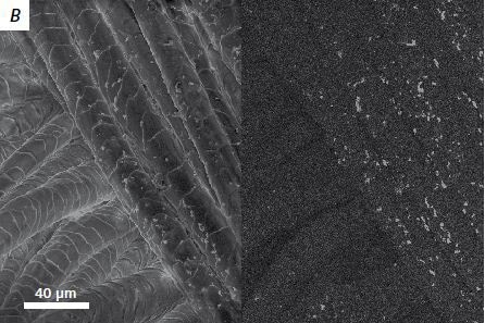
Figure 5. b) Low magnification Ag nano-particle coated natural fibers, imaged with Inlens SE (left) and EsB (right) detectors at 80 Pa and 10 kV, Sample: courtesy of SBUK and Dr. F. Simon, Leibniz Institute of Polymer Research Dresden, Germany.

Figure 5. c) Image shows medium magnification of filter paper, imaged at 80 Pa and 3 kV Inlens SE.

Figure 5. d) High magnification of Au/Pd thin film deposited on glass, imaged at 40 Pa and 5 kV, Inlens SE.
Both EsB and Inlens SE detectors are utilized to achieve material contrast and surface topography, and these two types of contrast are distinctly isolated.
Conclusion
These systems, based on over two decades of expertise with Gemini technology, provide ease of use, excellent resolution, and efficient detection. With the novel Gemini lens design, the resolution limits are pushed to lower voltages again, which results in adequate resolution across a broad voltage range.
Due to retractable pressure-limiting aperture and retractable detectors for the VP mode, excellent flexibility is realized for the electron microscopist. The Gemini lens is designed for sophisticated imaging at both low and high pressures, thus addressing real world sample requirements.

This information has been sourced, reviewed and adapted from materials provided by Carl Zeiss Microscopy GmbH.
For more information on this source, please visit Carl Zeiss Microscopy GmbH.