Sponsored by Gatan, Inc.Reviewed by Olivia FrostFeb 1 2023
“Photonic applications using the II-VI semiconductor zinc oxide (ZnO) are becoming increasingly prevalent, and research into even more uses is exploding, with hundreds of labs looking into the material’s unique properties.”1
One of the reasons why ZnO is finding increased popularity as a potential replacement for gallium nitride and other semiconductors is the fact that it is environmentally benign. ZnO is also bio-compatible, meaning it would be extremely suitable for future medical applications.
ZnO is transparent at wavelengths within the visible section of the electromagnetic spectrum, and it is opaque at ultraviolet wavelengths. It has pyroelectric and piezoelectric characteristics and has been produced in a wide range of different forms to suit specific optoelectronic applications.
A form produced by a vapor growth process has been analyzed utilizing Electron Backscatter Diffraction (EBSD) in the Scanning Electron Microscope (SEM).
As shown in Figure 1, both infrared (IR) and visible light can be transmitted through crystals of materials such as Magnesium Aluminate (MgAl2O4), Alumina (Al2O3), and Magnesium Fluoride (MgF2).
With recent developments in materials formation, these materials can now be formed in polycrystalline form while still being able to retain their transmittance properties. The cost of fabrication for polycrystalline ceramic materials is a great deal lower than that of single-crystal materials.
As these polycrystalline ceramics can be fabricated in highly dense compacts, pore formation can be prevented. This increases transparency as pores are deleterious to the transmission of light.
Ceramics tend to have high strength and hardness, along with good damage and thermal shock resistance. These materials are, therefore, well-suited for windows and protective dome applications.
In-depth knowledge of the factors affecting the light-scattering properties of polycrystalline materials is required to produce materials with good IR transmission. Grain size, or more specifically, grain boundaries, is one of these factors. Previous studies2,3 have suggested that the transparency in MgF2 and Alumina can be improved by reducing the grain size.
The crystallographic orientation of the constituent crystals, or texture, is another factor that influences the transmittance.4 The microstructural characteristics of materials can be characterized effectively using EBSD.
Furthermore, the chemical composition (which is important to measure as it affects performance) of these materials and the spatial distribution within the microstructure can be characterized by Energy Dispersive Spectroscopy (EDS).
This article describes examples of EDS and EBSD analysis of these materials.
Zinc Oxide5
Well-faceted ZnO microfibers with periodic junctions are shown in Figure 2. The microfibers were fabricated using an evaporation and deposition process, and they include spacings between the junctions, which range from 5–30 µm.
The spacing can be regulated by controlling the growth conditions. The characterization of these materials was carried out using various techniques, including photoluminescence (PL) microscopy, EBSD, scanning electron microscopy (SEM), energy dispersive X-Ray (EDS) analysis, and X-Ray diffraction (XRD). EBSD was particularly important in characterizing the anisotropic growth mechanism of the fibers.
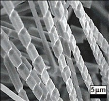
Figure 2. ZnO microfibers with periodic junctions with 6.2 μm spacing. Image Credit: EDAX
Figure 3 shows an anisotropic microfiber growth model. This was later confirmed by EBSD measurements on various fibers. Figure 4 shows an example of the EBSD measurements. EBSD was used to carry out orientation measurements along the length of the fiber. Upon analysis of individual orientation measurements, the fibers were found to be single crystals.
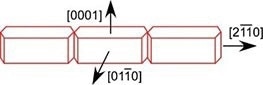
Figure 3. Microfiber anisotropic growth model. Image Credit: Gatan Inc.
Pole figure analysis of the data confirmed that the growth direction of the fibers is <2110>, the “side” surfaces are {0001} planes, and the top and bottom surfaces are {0110} planes. The base of the fiber is formed by fast growth along the <2110> direction and then slow growth along the c-axis [0001], forming regular prisms.
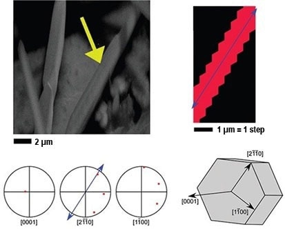
Figure 4. EBSD measurements and pole figure analysis. Image Credit: EDAX
As shown in Figure 5, photoluminescence studies revealed the correlation between the structure and the optical character of the fibers. The photoluminescence behavior means the modulated fibers may act as microscale waveguides, and the creation of microscale light-emitting arrays and bar codes for biotechnology and electronics may become possible.
EBSD can also be used for the characterization of other forms and applications of ZnO. For example, on polycrystalline ZnO varistors,6 powder compact specimens,7 single-crystal nanoscrews,8 and tetrapods where each leg of the tetrapod is a single crystal.9
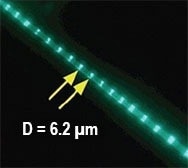
Figure 5. Photoluminescence micrograph for the type of fibers shown in Figure 2. Image Credit: EDAX
Magnesium Fluoride
Magnesium Fluoride (MgF2) possesses a tetragonal crystal structure. Wen and Shetty2 revealed that grain size impacts optical transmittance in polycrystalline MgF2. Figure 6 shows orientation maps of MgF2 in the as hot-pressed form and then annealed at different annealing temperatures.
EBSD was used to provide the orientation data in addition to the characterization of grain size in these materials. The orientation maps are generally referred to as orientation imaging microscopy (OIM™) maps.
Accurate grain size measurements using traditional light microscopy are difficult to obtain due to the ability of these materials to transmit light, which reduces the reflective grain boundary contrast.
Furthermore, the spatial resolution required to resolve the microstructure at the smaller grain sizes is higher than light microscopy can offer. From the OIM maps, it is evident that increased grain growth is facilitated by higher annealing temperatures.
Figure 6 shows the polycrystalline MgF2 samples for which optical transmittance measurements were performed at different wavelengths. Figure 7 shows the graph in which the results are plotted as a function of grain size.
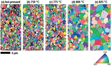
Figure 6. Color-coded orientation maps of polycrystalline MgF2 after a) hot-pressing and after b-e) annealing for one hour at the temperatures indicated. Image Credit: Wen and Shetty, 2009; Naval Air Warfare Center AD.
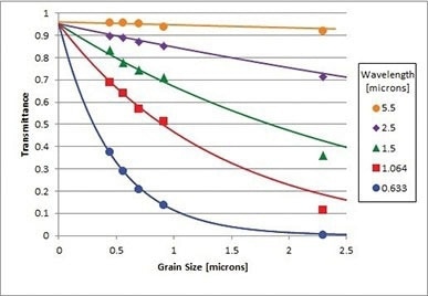
Figure 7. Optical transmittance of polycrystalline MgF2 as a function of grain size at five different wavelengths. The solid lines are from an analytical approximation. Image Credit: Apetz and van Bruggen, 2003.
Magnesium Aluminate Spinel
Spinels are traditionally referred to as red gemstones. However, in modern scientific literature, spinels refer specifically to crystals of magnesium aluminum oxide (MgAl2O4) or sometimes a class of minerals with a cubic crystal structure and specific chemical formula. Over a wide range of wavelengths, MgAl2O4 crystals are transparent.
The effect of changes in chemical composition across grain boundaries in a fine-grained spinel can be studied using EDS in the transmission electron microscope (TEM).10 Additional data on the grain boundary character distribution can be obtained using the SEM and EBSD.
The microstructure of MgAl2O4, after being hot-pressed and subsequently annealed, is shown in Figure 8. The figure was constructed based on EBSD scan data on the sample.
The color in the map correlates with their crystallographic orientation relative to the sample normal, and the hue is produced by mapping the quality of the corresponding diffraction pattern at each point in the OIM scan to a grayscale.
Results of the EBSD data analysis show that there was very little preferred orientation of the constituent crystals, and the misorientation at the grain boundaries was also random. The role of grain boundaries and sub-grain boundaries on the formation of microstructure in the materials has been studied by Ting and Lu11 using selected area diffraction in the TEM.
EBSD is an ideal tool for further researching grain boundaries in these materials, as analyzing many boundaries at one time is fairly easy, and therefore statistical analysis of grain boundary misorientation is far simpler.12
Figure 9 presents two EDS spectra, one corresponding to a hot-pressed sample and another to the hot-pressed and annealed sample in Figure 7. It is evident from the spectrum that the ratio of Mg/O and Al/O gradually decreases following annealing.
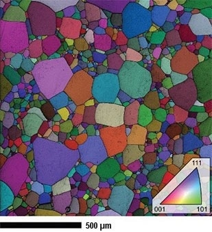
Figure 8. Orientation map overlaid on an intensity map based on EBSD pattern quality on a hot-pressed sample MgAl2O4 sample. Image Credit: EDAX
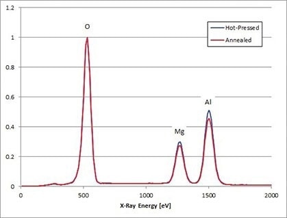
Figure 9. EDS spectra from a hot-pressed sample MgAl2O4 sample and a hot-pressed and annealed sample. Image Credit: EDAX
Alumina
Interestingly, the texture is one of the parameters influencing the transmittance performance of ceramic materials.4 The forming process of hot-pressed powder compacts is isotropic, and therefore, these materials do not exhibit much texture. However, some of these materials were observed to have some texture.
The microstructure of a hot-pressed transparent alumina sample shown in Figure 10 with a corresponding inverse pole figure shows the preferred orientation. The average grain size of the material was roughly 300 nm and the scan area consists of 1650 individual grains.
This number of grains should offer a reasonable evaluation of the texture.13 The texture is relatively weak; the highest intensity is nearly two times random for the c-axes to be aligned with the sample normal.
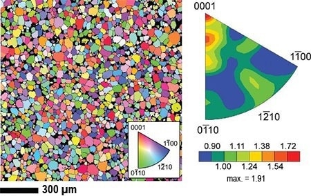
Figure 10. Orientation map and corresponding texture for a hot-pressed Al2O3 sample. Image Credit: EDAX
Conclusion
In the optical material industry, there are a number of exciting new research areas, both in terms of developing new forms of existing materials systems and developing new materials.
In-depth knowledge of the development of microstructure and its function in optoelectronic performance is important for enhancing the performance and fabrication of these materials, as well as their development into new fields of technology and applications.
EDS and EBSD serve as ideal tools for characterizing the aspects of microstructure and achieving insights on linking the properties with the microstructure.
References
- L Savage (2010). Making electro-optical sense with Zinc Oxide” Photonics Spectra 44(2): 47-49
- T.-C. Wen and D. K. Shetty (2009). Birefringence and grain-size effects on optical transmittance of polycrystalline magnesium fluoride.” Proceedings of the SPIE - Window and Dome Technologies and Materials XI, 7302: 73020Z-1- 73020Z-6
- R. Apetz and M. P. B. van Bruggen (2003). “Transparent Alumina: A Light-Scattering Model.” Journal of the American Ceramic Society, 86: 480-486.
- C. S. Chang and M.-H. Hon (2003). “Texture effect of hot-pressed magnesium fluoride on optical transmittance” Materials Chemistry and Physics 81: 27-32
- L. Huang, S. Wright, S. Yang, D. Shen, B. Gu and Y. Du (2004). ZnO well-faceted fibers with periodic junctions”” Journal of Physical Chemistry B 108: 19,901-19,903
- C. Leach (2005). ““Grain boundary structures in zinc oxide varistors”.” Acta Materialia 53: 237-245
- Y. J. Kim, D.-W. Kim, S. J. Ahn, H. S. Kim and S. Ahn (2003). ““Study on the non-linear property of abnormally grown grain ZnO”.” Materials Chemistry and Physics 82: 410-413
- L. Liao, J. C. Li, D. H. Liu, C. Liu, D. F. Wang, W.Z. Song and Q. Fu (2005) “Self-assembly of aligned ZnO nanoscrews: growth, configuration and field emission.” Applied Physics Letters, 86: 083106-1-083106-2.
- B.-B. Wang, J.-J. Xie, Q, Yuan and Y.-P. Zhao (2008) “Growth mechanism and joint structure of ZnO tetrapods.” Journal of Physics D, 41: 102005-1-102005-6
- N. Nuns, F. Béclin and J. Crampon (2005). “Space charge characterization by EDS microanalysis in spinel MgAl2O4.” Journal of the European Ceramic Society, 25: 2809-2811
- C.-J. Ting and H.-Y Lu (1999) “Hot-Pressing of Magnesium Aluminate Spinel – II. Microstructure Development.” Acta Materialia, 47: 831-840
- V. Randle (2004). ““Application of electron backscatter diffraction to grain boundary characterisation”.” International Materials Reviews 49: 1-11
- S. I. Wright, M. M. Nowell and J. F. Bingert (2007). ““A Comparison of Textures Measured Using X-Ray and Electron Backscatter Diffraction”.” Metallurgical and Materials Transactions A 38: 1845-1855

This information has been sourced, reviewed and adapted from materials provided by Gatan Inc.
For more information on this source, please visit Gatan Inc.