Sponsored by HORIBAJun 14 2018
The Scanning Electron Microscope (SEM) is an instrument that uses a focused beam of electrons to scan a rectangular area of the tested specimen (called raster scanning), and generate an image.
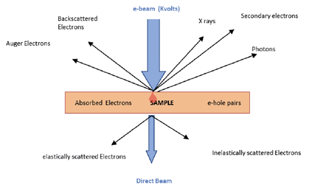
Interaction electron beam with sample
Electron guns come in two variants:
- The traditional thermionic emitters including filaments tipped with tungsten or lanthanum hexaboride.
- Tungsten field emission gun (FEG), both cold and warm, using a pointed-tip emitter which is kept at 2-7 kilovolts to induce a surface potential high enough to cause emission of field electrons in the form of a beam – which has a smaller size and greater coherence, besides being three or less orders higher in current density (also measured as brightness).
| Filament |
W-tungsten |
LaB6 |
FEG (Schottky) |
Cold FEG |
| Source Size |
30-50 µm |
5-50 µm |
15 nm |
3 nm |
| Temperature (oC) |
1700-2400 |
1500 |
1500 |
Ambient |
| Service |
Inexpensive |
Expensive |
Expensive |
Expensive |
| Vacuum (Torr) |
10-5 |
10-7 |
10-10 |
10-10 |
| Lifetime |
180.200 |
>1000 h |
>1 year |
>1 year |
| Brightness |
106 |
107 |
108 |
109 |
| Emission Current (µA) |
100-200 |
50 |
50 |
10 |
| Delta E/E |
2.5 eV |
1.5 eV |
1 eV |
0.25 eV |
The electron energy depends on the voltage, and varies from 1 Kev to 50 KeV
Current (A): Number of electrons/unit of time
1 amp = 1 coulomb/sec 1 coulomb, or approximately 6 x10¹⁸ electrons
For instance, a measured current of 10-9 A to 10-12 A corresponds to around 6 X 10⁶ to 6 X 10⁹ electrons/second.
Environmental Scanning Electron Microscope
The Environmental Scanning Electron Microscope (ESEM) is a modified version of SEM which can image samples in either the wet state or contained in low vacuum or in a gas with adequate resolution and quality. This is particularly useful in producing images from biological specimens that cannot withstand conventional electron microscopy because of its high vacuum. Transmission EM requires very thin specimen slices, about 100 nm.
Biological samples must be first fixed chemically, then dehydrated and embedded in a resin polymer so that they are stable enough for such thin sections to be prepared. For sufficient contrast, it may be necessary to treat organic polymers, biological sections or other materials of this type with labels containing heavy atoms.
The greatest use of ESEM is in imaging uncoated, non-metallic or biological specimens. Argon or other gases are typically present around the specimen so that a pressure higher than 500 Pa can be achieved, whereas a vacuum of approximately 10-3 to 10-4 Pa is required for SEM imaging. At such a vacuum, non-conductive samples do not need to be prepared first, nor do hydrated samples require charging beforehand.
Transmission Electron Microscope (TEM)
A Transmission Electron Microscope (TEM) uses an anode-accelerated electron beam, with a potential difference of about +100 keV (40 to 400 keV) between the positive and the negative electrodes, which is then concentrated using electrostatic and electromagnetic lenses before transmission through the specimen.
Some degree of scattering occurs at the specimen because it is only partly transparent to light. The scattering leads to a difference in the emerging electron beam which conveys much data about the specimen structure and is magnified by the objective of the microscope.
This is called the image and shows variation over space which is converted to a visible image by being projected onto a viewing screen that is fluorescent, being coated with a phosphor or with a material like zinc sulfide which scintillates.
Another method is to make a photographic record using a photographic film or plate directly exposed to the emerging magnified beam. A third method is to couple a high-resolution phosphor to a digital camera sensor using a lens system or a fiberoptic light guide, so that the camera detects the image. This can then be projected to a computer or a monitor as required.
A TEM has the advantage of being able to produce images with a resolution of about 50 picometers and which are magnified about ten million times, compared to a conventional light microscope which resolves images only to approximately 200 nanometers by diffraction, and magnifies them less than 200 times.
When compared to SEM, a TEM has a resolution which is higher by one or more orders of magnification. On the other hand, an SEM can produce images of samples which are quite large (several centimeters across) because it uses surface scanning processes rather than directing the electron beam through the sample. Moreover, an SEM can be designed and its settings adjusted to image a sample to a higher depth of field, generating an image that represents the sample shape in three dimensions.
Scanning Transmission Electron Microscope
The Scanning Transmission Electron Microscope (STEM) scans the specimen surface in a rectangular (raster) pattern using a focused beam of electrons from a probe. The specimen must be prepared by making extremely thin slices to ensure that electrons are able to pass through and be scattered by the specimen.
This emerging beam is detected. This technique offers the same high resolution as TEM, the difference being the timing of the beam focusing, which is before the beam strikes the specimen in STEM but occurs after this event with TEM.
Focused Ion Beam
A Focused Ion Beam, or FIB, is used very often to analyze the structure of semiconductors, materials in materials science, and biological specimens. It ensures analysis, deposition, and ablation of materials in a manner specific to the site. The equipment used is similar to an SEM but uses a focused beam of gallium ions instead of electrons, and thus the specimen is destroyed during FIB.
The ions possess high energy and thus when the beam is incident on the sample it strikes off atoms from the surface, as well as causing some gallium atoms to stick to the surface, within the first few nanometers. Thus the surface of the specimen becomes irregular in structure.
A combined FIB-SEM system is equipped with columns to send both electron beam and ion beams. Thus either of them can be used to analyze a single feature of a specimen. Firstly, a beam of gallium ions is directed on the surface to find the defect or the feature to be studied. Secondly, the electron beam (from the inbuilt SEM) is used to image the specimen.

This information has been sourced, reviewed and adapted from materials provided by HORIBA.
For more information on this source, please visit HORIBA.