Laser beam welding is a modern material joining technique that uses a high power density laser to heat and fuse two materials together. Laser-based methods can achieve higher speeds, narrower welds and are easier to automate than traditional welding techniques.
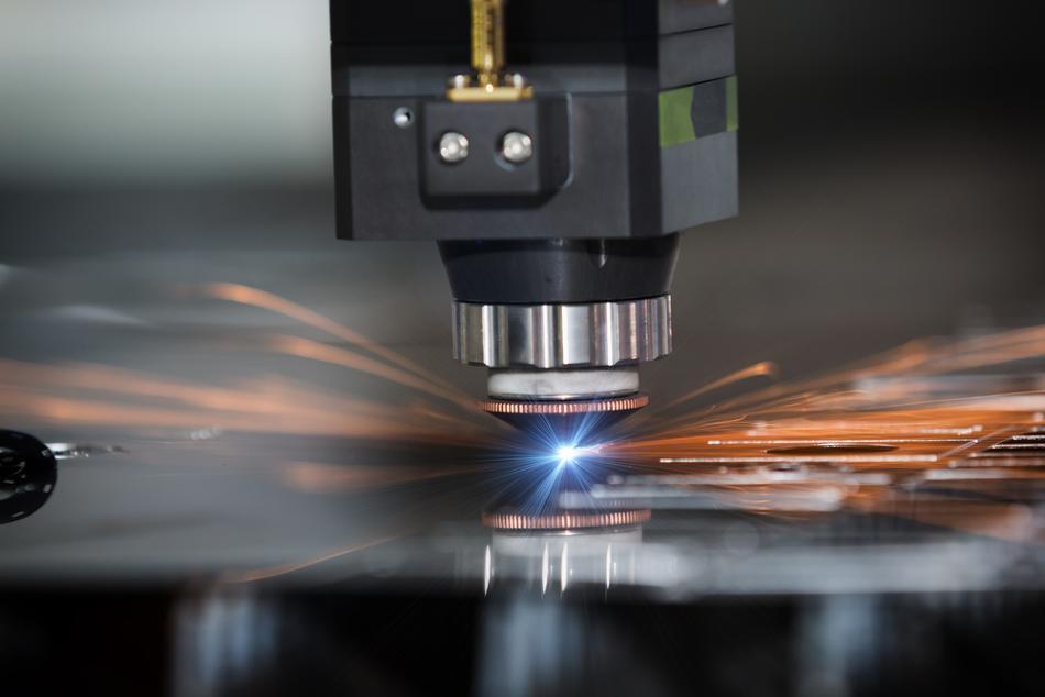
Image Credit: Aumm graphixphoto / Shutterstock.com
As with traditional welding techniques, materials are melted in the weld zone, although laser-based techniques use quicker heating and cooling cycles (Figure 1).
These rapid thermal cycles are a potential cause for concern due to cracks forming. Cracks form due to thermal stresses and changes in the microstructure, which produce undesirable or inhomogeneous mechanical properties. This area is known as the heat-affected zone (HAZ). Therefore, high-resolution and high-precision mechanical property data in the HAZ is very important for ensuring weld quality and optimizing laser operating parameters.
Laser beam welding is used widely in the electronic and automotive industries where welds need to be small, rapid, precise and highly automated. The inherent size of the laser spot size (≈200 μm) that is used during laser beam welding produces a small HAZ.
This is often too fine to be characterized properly by optical microscopy and macro/micro indentation techniques, such as Rockwell and Vickers. Therefore, a combination of nanoindentation and scanning electron microscope (SEM) based characterization techniques are better suited to the length scale of laser beam welds.
This article presents a combined nanoindentation mapping and electron backscatter diffraction (EBSD) study of 410 stainless steel laser cladding on a 4140 steel substrate to evaluate changes in mechanical properties and microstructure as a result of the joining process.
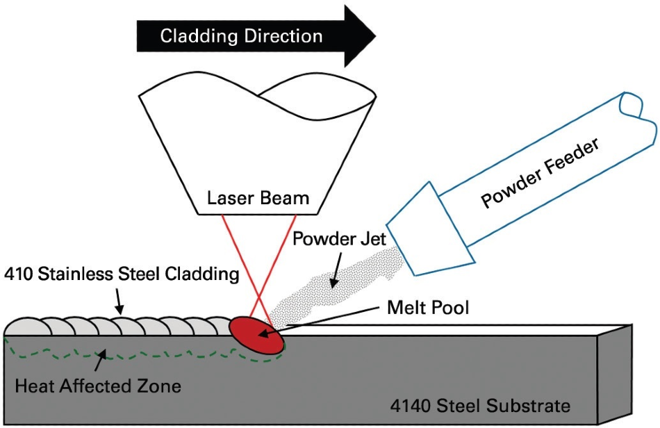
Figure 1. Schematic of laser cladding of 410 stainless steel onto a 4140 steel substrate. The laser beam weld produces a heat affected zone resulting in altered mechanical behavior and microstructure at the weld interface. Image Credit: Bruker Nano Surfaces
Experimental
Bruker’s Hysitron® TI 980 Tribolndenter®, equipped with a diamond Berkovich probe, was used to conduct nanoindentation experiments. A series of quasistatic accelerated property mapping (XPMTM) grids with indent spacing of 500 nm over a square distance of 34 μm x 34 μm, at 400 μN force, were carried out to identify the nanomechanical behavior of the weld interface (Figure 2).
EBSD experiments were conducted using an FEI Versa 3D SEM equipped with a Hikari EBSD detector supplied by EDAX to study the microstructural changes in the steel due to the laser weld. EBSD maps were gathered at 20 keV accelerating voltage, with a lateral step size of 200 nm.
To prepare the surface of the specimen for EBSD analysis, a final polishing step of 50 nm colloidal SiO2 was used. To ensure the nanoindentation and EBSD areas were well aligned, a fiduciary box marking was cut around the area of interest using the focused ion beam with Ga+ ions at 30 keA accelerating voltage and 1 nA beam current.
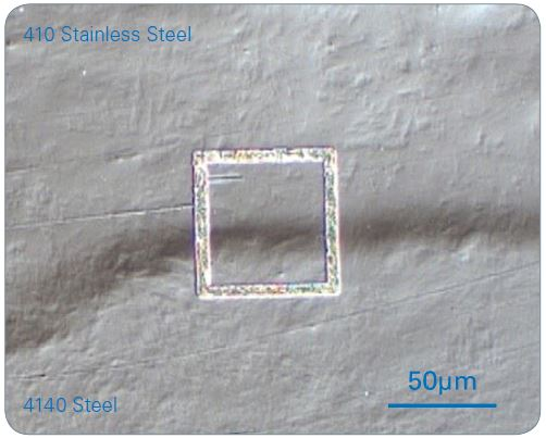
Figure 2. An optical micrograph of a cross-section of a 410 stainless steel/4140 steel laser beam welded interface. Nanoindentation was carried out within the focused ion beam (FIB) ablated square. Note: The nanoindentation grid is not visible. Image Credit: Bruker Nano Surfaces
Results and Discussion
Figure 3a shows a 2D modulus map of the welded interface. No spatial variation in elastic properties across the weld was evident. The average reduced modulus was 218.5 GPa ±17.5 GPa (N = 4356 indents). The location of the indents within the FIB ablated square are shown in Figure 3b.
Figure 3c demonstrates the variation in hardness across the welded interface with the 410 stainless steel measuring ≈8 GPa and the 4140 steel measuring ≈5 GPa. It is also apparent that the hardness is slightly higher within the weld zone. This is a result of the rapid quenching of these martensite-hardened alloys.
These hardness and modulus maps are compared against the EBSD data in Figure 4. The EBSD phase content was measured to be almost completely alpha phase (~85%), with well-distributed cementite (8%) and martensite (~7%). Figure 4c shows the EBSD inverse pole figure (crystal orientation) map.
An image quality map with marked boundaries is shown in Figure 4d. Figure 4c indicates some changes in grain size, shape and relative orientation across the weld zone. The 410 stainless steel has slightly smaller and less elongate grains.
However, compared to 4140 steel substrate, it has much larger orientation changes between neighboring grains. Therefore, some of the hardness increase in the 410 can be attributed to a reduced grain size through the Hall-Petch relationship. This states that grain size is inversely proportional to yield strength (correlated to hardness).
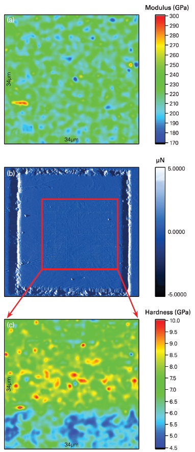
Figure 3. (a) 2D reduced elastic modulus map of the welded interface; (b) location of indents within the FIB ablated square from Figure 2; and (c) hardness map across the welded interface showing distinct differences between the 410 stainless steel and 4140 steel. Image Credit: Bruker Nano Surfaces
As well as different grain sizes, Figure 4d demonstrates an increased density of greater than 15o crystal misorientation grain boundaries within the 410 stainless steel, compared to the 4140 steel substrate. The higher angle grain boundaries are more effective at inhibiting dislocation motion.
The increased density of greater than 15o misorientation not only supports a difference in grain size between the types of material, it also suggests that transmission of dislocations to the neighboring grain is more difficult. This is due to increasing dislocation pile-up sizes and dislocation-dislocation interaction-based hardening.
Conclusions
The combined EBSD mapping and XPM nanoindentation showed correlated structure-property relationships in the stainless steel-steel weld zone, where high hardness was attributed to increased average grain boundary angle and decreased grain size.
Overall, the weld zone was relatively structurally homogenous, however, it possessed some areas of high local hardness. The speed of XPM mapping meant that nearly 5000 indents could be performed in approximately 30 minutes, with resolution and speed comparable to the EBSD mapping.
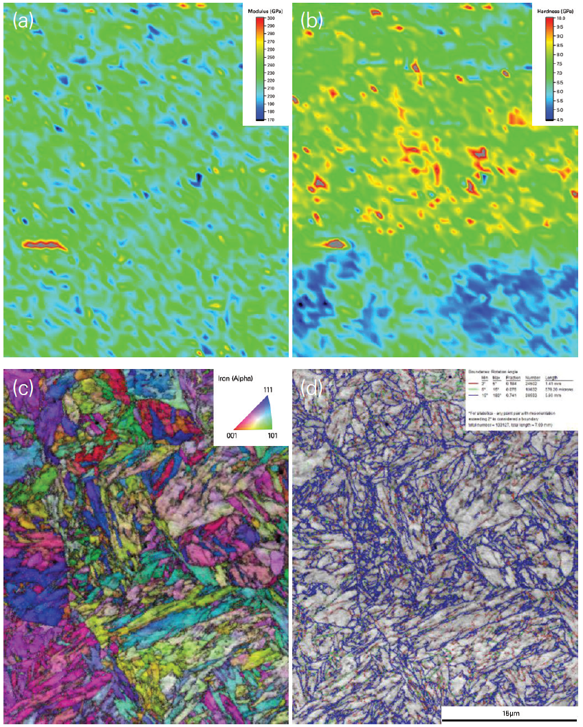
Figure 4. (a) Modulus map; (b) hardness map; (c) EBSD inverse pole figure map (i.e., crystal orientation); and (d) EBSD image quality map (i.e., crystal misorientation/grain boundary). Image Credit: Bruker Nano Surfaces
Acknowledgments
Produced from materials originally authored by Eric Hintsala*, Jared Risan* and John Haake+.
*Bruker
+Titanova, Inc.

This information has been sourced, reviewed and adapted from materials provided by Bruker Nano Surfaces. For more information on this source, please visit Bruker Nano Surfaces.