The Hysitron PI Envision SEM PicoIndenter offers advanced nanomechanical testing performance in a compact system engineered for effortless integration with a variety of microscopy platforms. Its upgradeable design supports long-term flexibility and evolving research demands.
Equipped with precise control and a library of over fifty interchangeable probe tips, PI Envision allows accurate mechanical characterization across a diverse material range, from delicate polymers to tough ceramics.
With sub-nanometer resolution in both displacement and force, the system supports a wide array of cutting-edge testing modes - including nanotribology, property mapping, high-throughput indentation, and thermal testing at elevated temperatures.
Its modular framework suits both standard and specialized applications, making it an ideal solution for multi-user labs and research environments focused on versatility, reliable data, and future scalability.
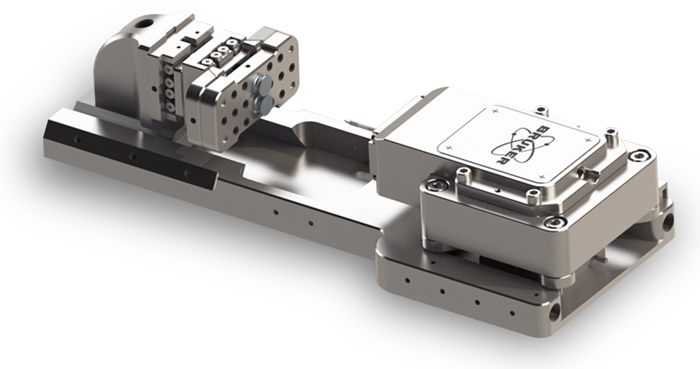
Image Credit: Bruker Nano Surfaces and Metrology
Hysitron PI Envision Delivers:
- Deliver precise material characterization with sub-nanometer resolution, supporting forces up to 250 mN and displacements up to 100 µm
- Enhance performance with optional modules for nanotribology, thermal testing up to 800 °C, and mechanical property mapping
- Encoded stage positioning and a rapid 78 kHz feedback loop ensure consistent, high-speed results in indentation, compression, tension, and fatigue tests
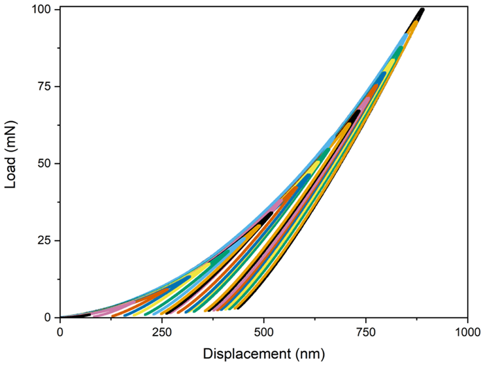
Load-displacement curve with high-load transducer option. Image Credit: Bruker Nano Surfaces and Metrology
Intuitive Operation for a Wide Range of Testing Modes
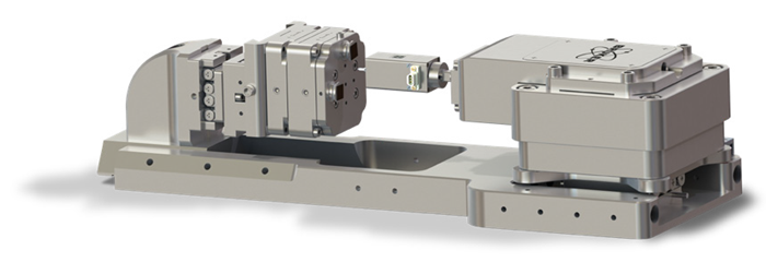
Image Credit: Bruker Nano Surfaces and Metrology
In-situ scratch testing using the nanoScratch module. Image Credit: Bruker Nano Surfaces and Metrology
Powered by Hysitron’s advanced transducer technology, the PI Envision delivers reliable, repeatable nanoindentation performance. Engineered for precision and ease of use, the system integrates several key features to streamline testing and improve efficiency:
- An encoded stage allows for accurate and repeatable positioning across a 12 × 12 mm travel range
- Dual sample holders simplify handling and increase flexibility for running varied experiments
- A large tip-to-mount standoff makes it possible to conduct room-temperature tests on samples up to 25 mm thick
Exceptional Value with an Easy Path to Future Upgradability
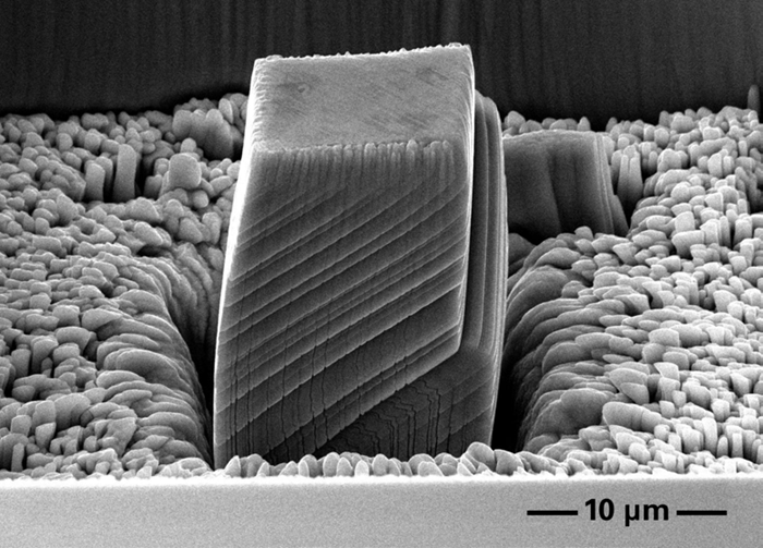
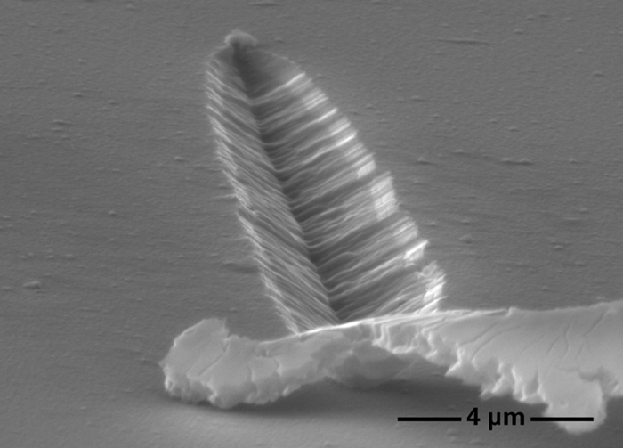
Micropillar compression with PI Envision. Image Credit: Bruker Nano Surfaces and Metrology
The PI Envision system comes standard with force capabilities up to 10 mN and a displacement range from 1 nm to 5 µm. Its base configuration supports a broad suite of standard and optional testing modes, including nanoindentation, compression, bending, direct-pull and push-to-pull tension, nanoDynamic, property mapping, and electrical characterization.
Performance can be further enhanced with system configurations that support forces up to 250 mN and an expanded displacement range of 1 nm to 100 µm. These advanced setups are compatible with additional modules, such as high-temperature testing up to 800 °C and nanotribological characterization.
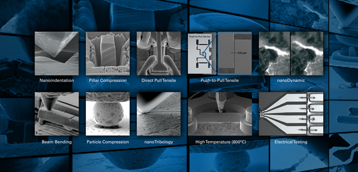
Image Credit: Bruker Nano Surfaces and Metrology
Hysitron PI Envision Specifications
Source: Bruker Nano Surfaces and Metrology
| |
| Max Force (transducer dependent) |
10 mN; 250 mN |
| Force Noise Floor (inside an SEM, 60 Hz) |
<0.4 μN |
Force Noise Floor (in ideal environment,
60 Hz, 10 mN transducer) |
<50 nN |
| Maximum Displacement |
5 μm; 30 μm; 100 μm |
Displacement Noise Floor
(inside an SEM, 60 Hz) |
<1 nm |
| Displacement Noise Floor (ideal environment, 60 Hz, 10 mN transducer) |
<0.1 nm |
| Machine Stiffness |
0.7 × 10⁶ N/m |
| Sample Positioning Range and Sensitivity |
12 mm × 12 mm × 16 mm (indentation axis); 1 nm encoder |
| System Size (base system, excluding SEM stage connecting adapter) |
55 mm × 32 mm × 191 mm (W × H × L); 460 g |
| Multi-Sample Mount |
Yes |
| Automated Indentation with Stage |
Large area: (>1 mm × >1 mm), no stitching |
| Tip Options |
Over 50 available, including diamond, sapphire, vanadium carbide, boron nitride, tungsten, and steel |
Hysitron PI Envision Modes and Capabilities
Source: Bruker Nano Surfaces and Metrology
| |
| Nanoindentation Testing |
Supports load-controlled, displacement-controlled, and open-loop for fundamental mechanical characterization |
| Compression Testing |
Enables intrinsic displacement-controlled testing of micropillars, nanoparticles, and other small-scale structures |
| Direct-Pull Tensile Testing |
Employs a gripper probe to apply stable, uniaxial tensile loads for accurate material response |
| Push-to-Pull (PTP) Tensile Testing |
Uniquely simplifies tensile testing of nanostructures such as nanotubes, nanofibers, nanowires, and thin films (patented by Bruker) |
| Electrical PTP Tensile Testing |
Enhances PTP testing with integrated four-point electrical measurements to study electromechanical coupling |
| nanoScratch Testing |
Simultaneously captures normal and lateral forces to evaluate friction, interfacial strength, and adhesion - ideal for semiconductor materials and coatings |
| Electrical Characterization |
Monitors changes in electrical properties during mechanical deformation; applicable to piezoelectric and other functional materials |
| High-Temperature Heating |
Enables mechanical testing - quasi-static, dynamic, and mapping - at elevated temperatures up to 800 °C |
| Property Mapping |
Rapidly generates high-spatial-resolution quantitative mechanical property maps |
| nanoDynamic Testing |
Applies oscillatory forces to continuously evaluate viscoelastic and fatigue properties at room and elevated temperatures |