Additive manufacturing, also known as 3D printing, has had a major impact on the contemporary design and production process.
First developed in 1988 with the aim of allowing for rapid prototyping, additive manufacturing enables the production of 3-dimensional physical objects via layer-by-layer deposition, directly from a file on a computer.
3D printing is vastly different from traditional subtractive machining – for example, CNC "computer numerical control" machining - which involves material being removed from the substrate in order to produce the final product.
Additive manufacturing offers numerous advantages over subtractive manufacturing. These include a reduction in waste, an increase in internal complexity, and no need for product-specific tooling. The process melt used in direct material deposition can, unfortunately, introduce defects, and this issue has historically limited the effectiveness of using 3D printers in prototyping applications.
These defects have a wide range of causes, including unanticipated thermal deformation, melt pool instability, energy source fluctuations, and environmental anomalies.1
Real-time monitoring is essential in minimizing scrap rates – essential if users are to take full advantage of additive manufacturing’s potential benefits. Monitoring is particularly vital in metal 3D printing, because of the exceptionally high melt points and expensive material requirements.
Fortunately, the high temperatures employed in metal 3D printing enable the integration of passive optical emission spectroscopy (OES). In order to appreciate the use of OES with a metal 3D printer, it is important to gain an overview of the technology itself.
Fundamentals of Metal 3D Printing
Two key methodologies are employed in modern direct metal disposition 3D printers: laser powder bed fusion (LPBF) and directed energy deposition (DED).2 These are illustrated in Figures 1a and 1b respectively.
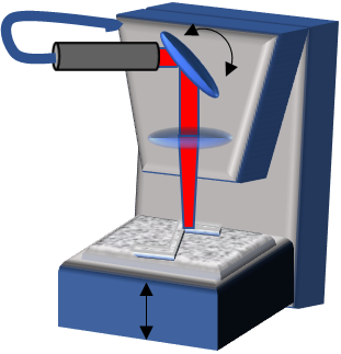
Figure 1a. Laser Powder Bed Fusion LPBF.
Both techniques utilize a high-power laser, such as a fiber or CO2 laser, to fuse powdered metal according to a pre-programmed pattern. This is done layer-by-layer in order to create the final product.
LPBF involves the complete platform being uniformly covered with a thin layer of powder, before being laser-scanned across the bed using an f-theta focusing lens and galvanometric mirrors. Once each layer has been fused, the platform is shifted down. This process is repeated until the construction of the final part is finished.
The DED, however, involves a laser being focused on a fixed location, while powder jets arranged at a suitable angle are used to intersect the laser’s focus. Here, the material substrate is situated on an X-Y-Z translation stage before being scanned underneath the laser, layer-by-layer, throughout the fabrication process.
DED processing is currently the most commonly used approach to the direct metal deposition because of its high throughput, larger build volume, and low waste. LPBF, however, is still employed in high precision applications, especially in cases where layering heights of under 250 mm are needed.
The most common choices for metal additive manufacturing materials are AlSi10Mg, Ti-6Al-4V, inconels (Ni-alloys), and steels (including stainless). This is the case for both LPBF and DED printers.
While each of these deposition methods is capable of processing any of these materials, DED is also capable of utilizing wire feed technology – something that LPBF cannot accommodate. Using a wire feed, DED printer heads are able to work with a much wider range of printer materials, while ensuring a lower price.
For instance, additive manufacturing grade 316 stainless steel powder will involve average costs per pound which are twice as high as 316 stainless steel wire. The only disadvantage to using a wire is that the system’s resolution will be limited by the thickness of the wire itself. This is typically on the order of 1 mm in diameter.
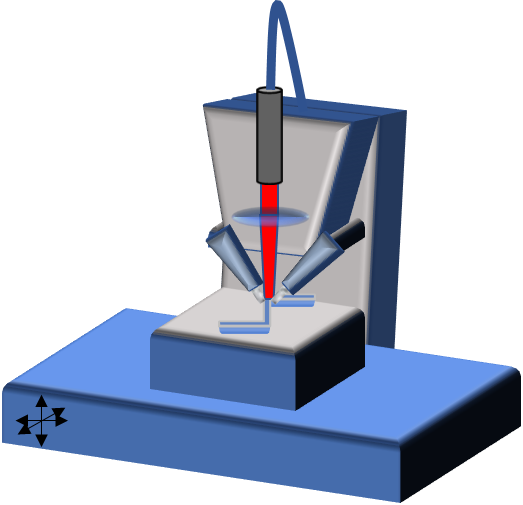
Figure 1b. Directed Energy Deposition DED.
OES in Additive Manufacturing
It is clear why OES is such a desirable tool for process monitoring when examining the geometry of the two key additive manufacturing processes for metal 3D printing outlined above.
Figure 2 displays an AvaSpec-3648-USB2 which has been integrated into a DED printing head.3 In this example, the light was collected via a fiber optic cable oriented at a 60-degree angle, relative to the laser's optical axis. Within this application, a team at the University of Brussels was utilizing OES to monitor the melt pool’s color temperature.
![Picture of fiber-optic cable and collection optics integrated into DED printing head [3].](https://www.azom.com/images/Article_Images/ImageForArticle_19408_15935826951826857.png)
Figure 2. Picture of fiber-optic cable and collection optics integrated into DED printing head3.
While the main aim of this study was to develop a non-contact control system capable of preventing excessive heat transfer in the substrate - therefore reducing material stress – the study also highlighted the way in which defects could be connected to the presence of oxidation.
It has also been shown that by monitoring the ratio of atomic emission lines, this can be directly linked to the likelihood of structural defects, as these are caused by changes in atomic concentrations.
A team at Pennsylvania State University confirmed a direct connection between vanadium and atomic titanium emissions and the formation of defects in Ti-6Al-4V.1
A group from the University of Michigan was also able to use OES to monitor chromium composition in H13 tool steel, using this for real-time material characterization, process optimization, defect detection and process control.4
Because of these studies, an increasing number of manufacturers are insisting on real-time monitoring for the detection of defects early in the production process.
Spectrometer Requirements
A spectrometer is used to collect OES data for additive manufacturing process monitoring will generally need superb spectral resolution, in order to properly differentiate between similar atomic species.
The AvaSpec-ULS4096CL-EVO from Avantes offers an ideal solution for this application, as can be seen in Figure 3. This spectrometer offers 0.05 nm resolution, working within the range from 200 nm to 400 nm using a 3600-groove density grating.
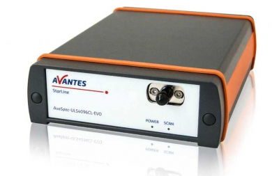
Figure 3. AvaSpec-ULS4096CL-EVO High-Resolution Spectrometer.
The AvaSpec-ULS4096CL-EVO also possesses a CMOS detector array, which is well suited for high light level applications (like the one described here) due to its improved dynamic range and linearity in contrast with CCD detectors.
Avantes' proprietary rapid electronic triggering, analog, and digital I/O capabilities and exceptional data transfer rates, ensure that the AvaSpec series offers seamless integration into a diverse array of existing high-speed inspection systems.
Each AvaSpec spectrometers is available as an OEM module, meaning that they can also be integrated into turnkey process control systems. These units are able to communicate via Ethernet, USB, and the native digital and analog input/output capabilities of the Avantes AS7010 electronics board, ensuring excellent interface capabilities.
The Avantes AvaSpec DLL software development package includes sample programs in Delphi, C#, C++, Visual Basic, MatLab, LabView, and a range of other programming environments, allowing users to easily develop code for use in their own applications.
Additionally, Avantes spectrometers have been designed with multiplexing or concatenation in mind, making them well suited for the multichannel operation. Each spectrometer in the system can be optimized for spectral resolution over a small range (generally 200 nm – 300 nm), allowing the OES signal to be evenly split amongst them using a multichannel fiber optic bundle.
This approach enables multiple redundant channels or ultra-high-resolution configurations across a far broader range. Avantes also supplies multi-channel configurations as individual modules, or these can be integrated into rackmount systems (Figure 4).
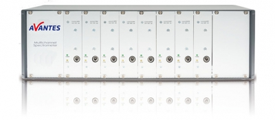
Figure 4. Avantes Multichannel Rackmount System.
When a spectrometer is integrated into a 3D printer head, it is vital that the fiber-optic cable selected is suitable for the specific environmental conditions it is to be used within. In harsh manufacturing environments, for example, metal-jacketed fiber optic cables offer the most protection from damage, but these do suffer from reduced flexibility.
It is important to take into consideration the system’s mechanical constraints, such as cable routing and management when choosing a fiber optic cable. In certain cases, fiber assemblies able to withstand temperatures as high as 500 °C may be essential, particularly if the fiber tip is operated in close proximity to the melt pool.
Avantes can provide a wide range of fiber cable configuration options, ensuring that the ideal solution for a particular integration application can be easily found.
References and Further Reading
- Nassar, A.R., Spurgeon, T.J. and Reutzel, E.W., 2014, August. Sensing defects during directed-energy additive manufacturing of metal parts using optical emissions spectroscopy. In Solid Freeform Fabrication Symposium Proceedings (pp. 278-287). Austin, TX: University of Texas.
- Montazeri, M., 2019. Smart Additive Manufacturing: In-Process Sensing and Data Analytics for Online Defect Detection in Metal Additive Manufacturing Processes.
- De Baere, D., Devesse, W., De Pauw, B., Smeesters, L., Thienpont, H. and Guillaume, P., 2016. Spectroscopic monitoring and melt pool temperature estimation during the laser metal deposition process. Journal of Laser Applications, 28(2), p.022303.
- Song, L. and Mazumder, J., 2011. Real time Cr measurement using optical emission spectroscopy during direct metal deposition process. IEEE Sensors Journal, 12(5), pp.958-964.

This information has been sourced, reviewed and adapted from materials provided by Avantes BV.
For more information on this source, please visit Avantes BV.