As the development of contemporary materials has continued to advance from the macro scale to nanoscale, the requirement for sophisticated microscopy techniques has increased dramatically. Scanning electron microscopes (SEMs) are considered to be one of the most versatile and powerful tools for scientists because of their large depth of field (in comparison to optical microscopes), great spatial resolution (high-magnification), and the capacity for chemical composition analysis via several types of spectroscopy.
In several instances, visualization of specimen topography, microstructure, or establishing the cause of failure is achieved easily through a single image. Yet, it is often necessary to set up a multidimensional approach to be able to answer the appropriate question about material properties that will steer future technological progress.
This is where SEM provides unparalleled flexibility through the addition of an assortment of electrical, mechanical, and chemical test equipment making the instrument a self-contained ‘nano-laboratory.’ This article will detail numerous developments in SEM technology that enable new and more flexible approaches to the analysis of novel systems, such as Li battery-related materials, nanostructured and nanoporous materials, as well as unique approaches to 3D analysis in SEM.
From Macro to Nano – Seamless Navigation and Cross-Referencing
One of the requirements vital to researchers is the ability to connect microstructural defects or features to its micro and nanostructural properties. This could be key to understanding and improving upon the current material design. JEOL has recently integrated a ZEROMAG feature across all SEM platforms. This feature enables a snapshot of the specimen (optical image) to be taken by the user prior to SEM observation and then maneuver to a region of interest based on this image.
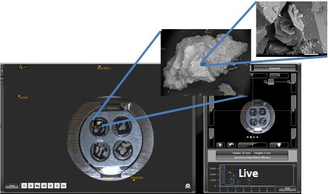
Figure 1. Seamless navigation and subsequent imaging and analysis via ZEROMAG function.
Furthermore, the user can magnify the area to the requisite feature size and observe and chemically analyze the location with the SEM while retaining the optical image tag (see Fig. 1). This is remarkably useful for the observation of multiple specimens or multiple locations on the same specimen.
Furthermore, an integrated Energy Dispersive X-Ray Spectroscopy (EDS) system can now tag these locations with chemical analysis and offer real-time compositional data as the multiple samples or multiple locations on the specimen are scanned.
Environmentally-Sensitive Materials Investigation
Multiple classes of modern materials demand preparation and subsequent analysis without air exposure due to potential oxygen or moisture-related reactivity. The most dominant technologically related class of materials is Li-based layered foils (positive electrode, electrolyte) for battery applications. Just a few minutes of exposure leads to the growth of an oxide layer that alters the view of the original material microstructure when working with Li. Therefore, JEOL has successfully developed an air-isolated transfer system compatible across it specimen preparation equipment (Cross-section Polisher [1], which uses a broad argon ion beam to prepare immaculate specimen cross-sectional surfaces). Additionally, this system is also compatible with a range of SEM and EPMA instruments (Fig. 2).
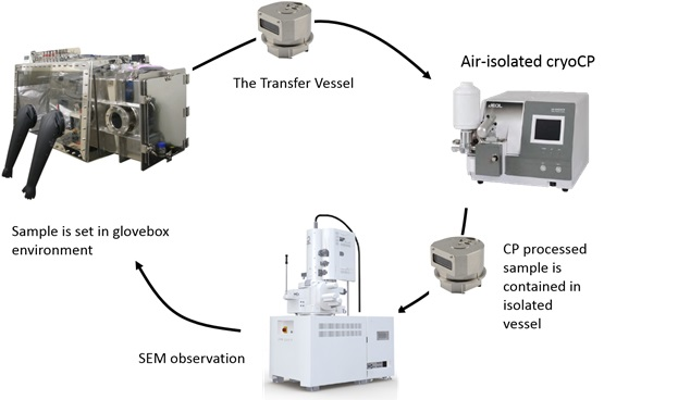
Figure 2. Specimen processing for air isolated workflow – the specimen is shuttled in a specially designed sealed transfer vessel that is compatible with both sample preparation equipment (ion polisher) and SEM and can be re-sealed for any further processing.
The transfer system is made up of a sealed capsule with a dovetail design that can be packed with a specimen in a glove box, sealed, then transported into either specimen preparation equipment and/or SEM without the risk of any environmental exposure. Subsequently, the sealing mechanism is only opened and re-sealed if required while under vacuum, therefore, avoiding any air exposure. This enables observation of the different elements of Li-battery materials and layers with high fidelity while using the especially low accelerating voltage capability of JEOL FE-SEMs. Fig. 3 illustrates the positive electrode with LiCoO2 particles enclosed in the battery that was charged and discharged 5 times with and without air exposure. The images detail the growth of an oxide layer and structural mutations after air exposure.
The air-isolated capsule can be used for a diverse range of materials including extraterrestrial particle specimens, various chloride complexes, radioactive materials, and many more.
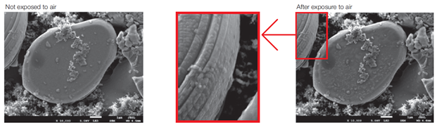
Figure 3. LiCoO2 particles in the positive electrode before and after air exposure. Clearly, air exposure introduces various artifacts affiliated with specimen reactivity with atmospheric oxygen.
Nanostructured Materials
Another exciting advance in SEM technology is the capacity to obtain extremely low voltage images that can assist the imaging and analysis of very thin surface layers. For example, nanoporous materials (zeolites, polymer membranes), atomic layer graphene or boron nitride sheets), as well as extremely electron beam sensitive materials.2 The extremely low voltage (JEOL FE-SEMs are able to image down to 10 V) is accomplished via a combination of progressive electron optics and detector design, Gentle Beam capability, as well as the unique JEOL NeoEngine capability.
The NeoEngine is the AI (artificial intelligence) system that tracks electron beam trajectories and alignment parameters and makes necessary adjustments as the user changes imaging and analysis parameters to ensure optimal imaging conditions at all times. The NeoEngine functions in the background, so that seamless operation is experienced by the user with minimal effort required to obtain images even at the extremely low voltages on difficult specimens. Fig. 4 exhibits examples of low voltage imaging that is now ordinarily achieved:
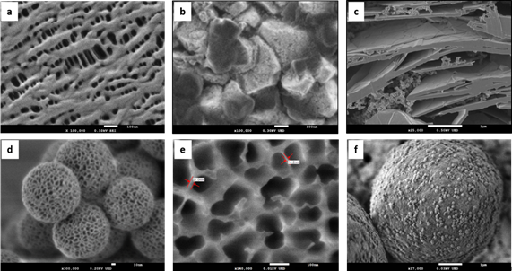
Figure 4. Examples of nanostructured materials imaged utilizing ultra-low accelerating voltage in FE-SEM. a) Polymer membrane used as a separator in Li batteries imaged at 100 V; b) Li battery positive electrode material imaged at 300 V; c) Cross-section of polymer sheet with graphene flakes and nano-particles imaged at 500 V; d) Nanoporous oxide particles imaged at 200 V; e) Anopore inorganic membrane (aluminum oxide) for filtration imaged at 10 V; f) Blue toner particles imaged at 30 V.
Utilizing SEM also allows for both the imaging of and EDS analysis of graphene layers in relation to the substrate, therefore furnishing a more direct analysis of graphene in its application-based environment. In contrast, TEM only permits the imaging of individual suspended sheets of graphene. Fig. 5 shows an example of EDS maps of graphene layers on Ni substrate, obtained at 1 kV and 5 kV.
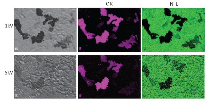
Figure 5. Low kV EDS mapping of graphene film on Ni substrate. Top: data acquired at 1 kV using probe current of 32 nA. Bottom acquired at 5 kV using a probe current of 4 nA.
When carrying out EDS analysis at low accelerating voltage, the beam–specimen interaction volume is reduced considerably, therefore, discrete maps of graphene and Ni components can be resolved. Moreover, in order to significantly reduce any buildup of carbon contamination that could obscure characterization on the surface of the sample, the mapping time was under 5 minutes. The high beam current setting in combination with a large-area detector (100 mm2) used for this analysis secured appropriate data collection for compositional interpretation even with a limited acquisition time at low kV.
3D Analysis of Surfaces
Long depth of field related to SEM imaging has conventionally appealed to the researchers because of the fundamental ability to generate a more three-dimensional representation of the specimen surface in contrast to optical microscopy. Although, there has been a concerted effort recently to take this capability even further, with various software and hardware solutions used to provide not only qualitative but also a quantitative representation of the 3D nature of specimen surfaces.
The proposed solutions range from simple composites of two or more stereo pair images (easily acquired through tilt series), Fig. 6a, to the actual redesign of detectors to obtain several images synchronously and merge those images to create a LIVE 3D representation of the specimen surface (Fig. 6b) that can be easily tilted, rotated, and manipulated by the user.
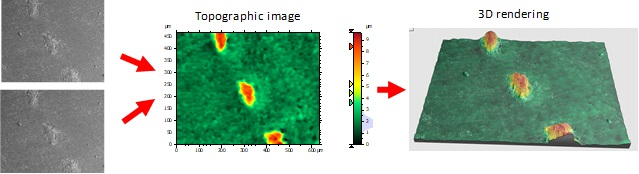
Figure 6a. Creating surface topography 3D representation through the acquisition of stereo pair of images. Rendering generated using MountainMaps (Digital Surf) software.
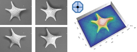
Figure 6b. LIVE 3D surface representation during SEM observation using a multi-segmented backscatter detector.
Conclusion
Utilization of state-of-the-art electron optics designs and unique detectors in combination with developments in graphic user interface software enables researchers to expand the use of SEM and offers innovative avenues for data integration and visualization. The detailed capabilities of 3D analysis, nanomaterials imaging at exceptionally low accelerating voltages, as well as seamless correspondence between optical and SEM images in combination with unparalleled ease of use, make SEMs indispensable tools in your laboratory toolkit.
Acknowledgments
Produced from materials originally authored by Natasha Erdman, Jennifer Misuraca, and Donna Guarrera from JEOL USA. Originally printed in Advanced Materials and Processes, April 2020.
References and Further Reading
- Erdman, N., Campbell, R., & Asahina, S. (2006). Precise SEM Cross Section Polishing via Argon Beam Milling. Microscopy Today, 14(3), 22-25. doi:10.1017/S155192950005762X
- D.C. Bell and N. Erdman (eds.) “Low Voltage Electron Microscopy – Principles and Applications”, RMS Wiley, 2012

This information has been sourced, reviewed and adapted from materials provided by JEOL USA, Inc.
For more information on this source, please visit JEOL USA, Inc.