In recent years, the use of pixelated detectors in scanning transmission electron microscopy (STEM) to obtain four-dimensional datasets has accelerated and achieved extraordinary traction. In particular, for the collection of a 2D convergent beam electron diffraction (CBED) pattern at each electron probe position throughout the course of a STEM scan: these pixelated detectors also facilitate so-called 4D STEM, as illustrated in Figure 1.
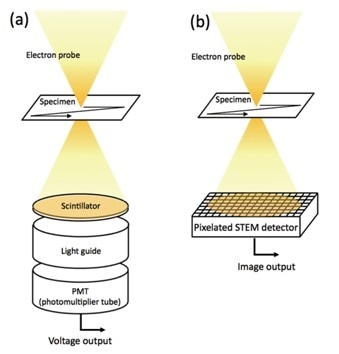
Figure 1. (a) Conventional STEM detector compared to a pixelated STEM detector (b). Image Credit: JEOL USA, Inc.
A multitude of signals can be realized in 4D STEM datasets; by applying virtual masks to the detector plane as well as modifying the camera length and convergence angle, it is possible to extract, for example, a corresponding bright field (BF), annular dark field (ADF), annular bright field (ABF), etc., STEM image.
In addition to more conventional imaging modes, differential phase contrast (DPC) STEM can be achieved with pixelated detectors, measuring the magnitude and direction of any incident beam deflection as a result of specimen interaction. Both phase (via ptychographic reconstruction) and strain information can also be extracted from 4D STEM datasets.
The JEOL 4DCanvas utilizes a pnCCD sensor: a direct electron detection CCD by PNDetector GmbH. With high frame rate capabilities and quantum efficiency of almost 100%, the 4DCanvas pixelated detector provides rapid, high-sensitivity 4D dataset acquisition. Particularly, when considering frame rates from 1,000 fps (full frame readout) – 7,500 fps (four-fold binning), a 256x256 pixel scan can be finalized in less than 10 seconds.
Corresponding dwell times of the electron probe range from 1 ms–133 ms. High frame rate capabilities are critical for 4D STEM datasets, as the detector speeds aim to approach those of traditional STEM image acquisitions.
Below, examples of a Lorentz and Ptychographic reconstructions are exhibited. Remarkably, the position of the 4DCanvas is below the viewing chamber, so simultaneous acquisition of 4D STEM datasets is made possible with the more traditional ADF STEM signals.
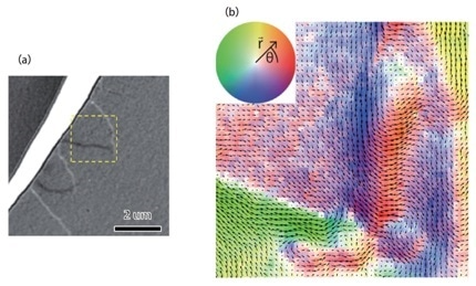
Figure 2. (a) Lorentz TEM image of a Ni film, detailing magnetic domain walls; (b) Map of the magnetic field of the same region in (a), acquired in DPC STEM. The deflection of the incident beam when passing through a ferromagnetic specimen can be captured in the CBED pattern recorded at probe position in a 4D STEM dataset. The magnitude and direction of this shift can be directly measured, as shown. Image Credit: JEOL USA, Inc.
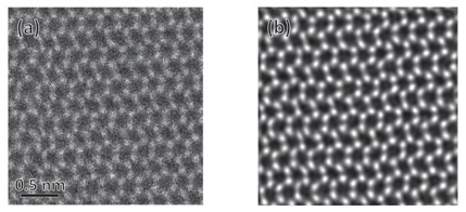
Figure 3. Graphene ADF STEM image (a), and after ptychographic reconstruction of a 4D dataset (b). Ptychography is an effective method by which to reconstruct a weak phase object, such as graphene. In this case, the two signals were acquired simultaneously. Image Credit: JEOL USA, Inc.
References
- R. Sagawa, JEOL News 52 (1) (2017) 53-57.
- R. Sagawa et al., Microsc. Microanal. 24 (Supp 1) (2018) 198-199.

This information has been sourced, reviewed and adapted from materials provided by JEOL USA, Inc.
For more information on this source, please visit JEOL USA, Inc.