JEOL designed the Monochromated JEM-ARM200F for researchers who need ultrahigh energy resolution EELS investigation of materials at the atomic scale. The monochromator includes a Spot-in-Spot-out double Wein filter, which maintains the electron beam's spot size and lattice resolution in STEM.
Key Features
Monochromator Double Wien Filter “Spot-In and Spot-Out system”
The spot beam from the Schottky source passes through the first Wien filter and an electrostatic lens, which together produce a focus with an energy dispersion of 12.3 μm/eV at the slit plane. At this point, the electron beam is monochromated by inserting a slit with selectable widths ranging from a few microns down to sub-micron scales. The second Wien filter then cancels the energy dispersion and creates an achromatic, stigmatic focus at the exit plane, resulting in a round probe at the specimen plane.
After monochromation, the beam returns to a spot configuration. The Wien filter, featuring a refined octopole design, generates a uniform dipole field. The system operates consistently across the full accelerating voltage range, as the accelerator is positioned after the monochromator and the axial potential of the monochromator remains constant.
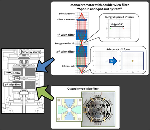
Image Credit: JEOL USA, Inc
Energy Resolution
With Several Widths of Slits at 60 kV and 200 kV (0.002 second and 0.1 second acquisition)
- With multiple acquisitions (0.25 μm slit)
Source: JEOL USA, Inc.
| |
60 kV |
|
200 kV |
|
| Slit width |
0.002 sec. |
0.1 sec. |
0.002 sec. |
0.1 sec. |
| 0.1 μm |
24 meV |
28 meV |
30 meV |
40 meV |
| 0.25 μm |
28 meV |
32 meV |
40 meV |
45 meV |
| 0.5 μm |
36 meV |
36 meV |
45 meV |
50 meV |
| 1.3 μm |
80 meV |
80 meV |
90 meV |
90 meV |
| 2.0 μm |
120 meV |
124 meV |
130meV |
130meV |
| 2.8 μm |
172 meV |
172 meV |
180 meV |
185 meV |
| 4.0 μm |
248 meV |
248 meV |
260 meV |
260 meV |
Zero-Loss Spectrum (ΔE: 14 meV @30 kV, 2 ms)
- With multiple acquisitions (0.25 μm slit)
The table below presents energy resolution measurements using slits of various widths at 60 kV and 200 kV. Zero-loss spectra were acquired with exposure times of 0.002 seconds and 0.1 seconds. The system achieved ultimate energy resolutions of 24 meV at 60 kV and 30 meV at 200 kV using a 0.1 μm slit and a 0.002-second acquisition time.
The comparison between 0.1-second and 0.002-second acquisitions shows only a slight reduction in energy resolution, indicating strong electrical and mechanical stability of the monochromator.
The figure shows the intensity profile of a zero-loss spectrum acquired at 30 kV with a 0.002-second acquisition time, demonstrating an energy resolution of 14 meV.
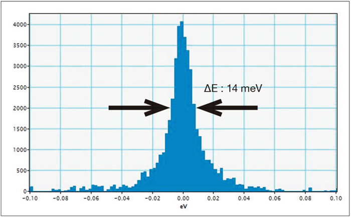
Image Credit: JEOL USA, Inc
Spatial Resolution
As shown below, raw HAADF-STEM images of Si [110] and their corresponding Fourier transforms were captured at 200 kV and 60 kV using different energy slit widths.
While some current loss is unavoidable due to the slit, the comparison confirms that lattice resolution in STEM remains unaffected by the monochromator. Power spectra obtained with both 4 μm and 0.25 μm slits display isotropic resolution. This demonstrates that, thanks to the double Wien-filter system, the monochromator maintains a round, monochromatic electron probe capable of achieving atomic resolution at any energy resolution, enabled by the "Spot-IN and Spot-OUT" design.
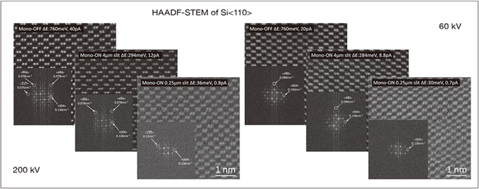
Image Credit: JEOL USA, Inc
Applications
Application 1: Phonon of hBN
- Vibrational spectrum of optical phonon from Hexagonal BN ΔE: 20 meV @30 kV
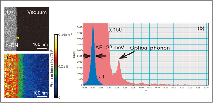
Low-loss EELS map of a hexagonal boron nitride (h-BN) with a monochromatic probe using a 0.1 μm slit. probe size = 1 nm, probe current = 10 pA, acquisition time for each pixel = 0.3 seconds. (a) shows the ADF-STEM image the mapping area. (b) shows the extracted low-loss spectrum from the edge of the specimen indicated with the framed yellow square in Fig. (a). This spectrum, measured with ΔE = 22 meV, showed a peak corresponding to an optical phonon at 170 meV. (c) shows the EELS map at the phonon energy. The phonon intensity was delocalized at the vacuum area > 100 nm beyond the sample edge due to the delocalization of inelastical scattering of electrons. Image Credit: JEOL USA, Inc.
Application 2: Surface Plasmon Resonance
- Surface plasmon resonance (Gold nano-rod) ΔE: 30 meV @60 kV
The surface plasmon resonance shown below was obtained using a gold nanorod and recorded at 60 kV with a 30 meV energy spread using the EELS map. The acquisition time per pixel was 0.15 seconds, and the probe current was 75 pA.
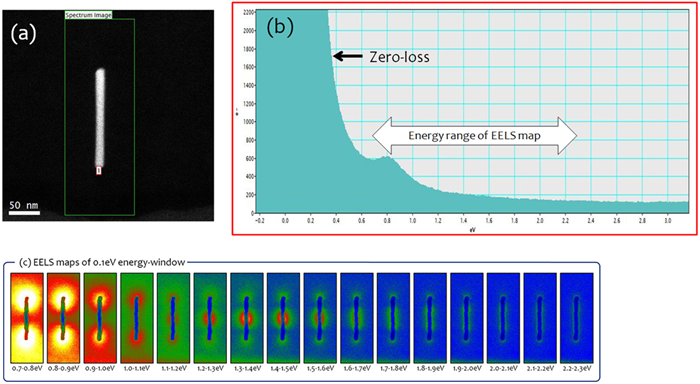
(a) HAADF, (b) low loss spectrum extracted from data cube of the spectrum imaging, (c) EELS maps of 0.1 eV energy width. Image Credit: JEOL USA, Inc.
Application 3: Vibrational Spectrum of a Molecule
- Vibrational spectrum of C-H stretching from ionic liquid ΔE: 30 meV @60 kV
EELS spectra magnified at ×1, ×10, and ×250 are shown below. In the ×250 magnified spectrum, a broad peak appears at –0.4 eV, marked by an arrow. This low-energy feature aligns with vibrational peaks in the IR spectrum (~3000 cm–1) and, based on theoretical calculations, is attributed to the C–H stretching vibrations of the [C2mim+] cations.
![(a) Structure of ionic liquid C2mim-TFSI, which is composed of [C2mim+] cation and [TFSI-] anion. (b) The EEL spectra, calculated and experimental IR spectra with energy scale](https://www.azom.com/images/equipments/EquipmentImage_9352_17479815190071579.png)
(a) Structure of ionic liquid C2mim-TFSI, which is composed of [C2mim+] cation and [TFSI-] anion. (b) The EEL spectra, calculated and experimental IR spectra with energy scale. Image Credit: Sample courtesy of Dr. Mizoguchi, The University of Tokyo