One of the most prominent challenges in the battery manufacturing process is the issue of contamination. Contaminants are a key concern at each stage of the process, from the production of the cathode, anode and battery cell to battery module assembly and testing.
The presence of contaminants in the battery can cause an array of problems, for example, reducing material usage efficiency, causing dangerous internal shorts or accelerating cell degradation.
Therefore, it is vital that material scientists can develop a comprehensive understanding of actual and potential contaminants throughout the battery manufacturing process.
A combination of scanning electron microscopy (SEM) and energy dispersive X-ray spectroscopy (EDS) can be employed in the investigation of both the structure and elemental information of contaminants in battery materials.
Battery contaminants typically exhibit a low concentration level, however, meaning that image acquisition can be rather time-consuming when studying these contaminants via traditional EDS.
This article showcases a rapid, straightforward approach to characterizing these contaminants using the Thermo Scientific™ Axia™ ChemiSEM - a novel SEM platform designed to bring much-needed speed and simplicity to materials microstructural analysis and defect discovery.
Large-Scale Navigation
The Axia ChemiSEM allows users to rapidly identify the presence of contaminants within a large field of view. This is due to the system’s comprehensive integration of different imaging modalities, for example, live quantitative elemental mapping and conventional SEM imaging.
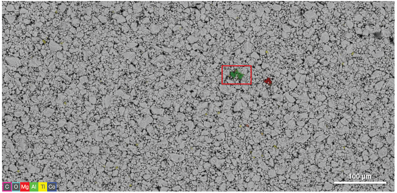
Figure 1. Large-scale navigation montage image obtained by collecting neighboring frames to generate a low magnification image for point-and-click navigation. 750 μm x 370 μm. Acquisition parameters: acc voltage 20 keV, beam current 0.13 uA. Image Credit: Thermo Fisher Scientific – Electron Microscopy Solutions
Figure 1 displays a navigation image acquired on the surface of a lithium cobalt oxide (LiCoO2) cathode using the Axia ChemiSEM. This large-scale overview of the sample included EDS data and was collected within 15 minutes.
A grayscale image with morphological information and featuring contrast based on backscattered electron signal cannot generally provide sufficient information to identify regions of interest for contamination analysis.
This limitation stems from a backscattered electron image providing a compositional contrast based on the atomic number. The compositional contrast between two different elements is often too similar to be reflected in grayscale.
In the example presented here, the quantitative elemental information provided by Axia ChemiSEM has already confirmed the presence and location of some foreign elements in the large-scale overview - magnesium (Mg), aluminum (Al) and titanium (Ti).
This large-scale overview functions as a navigation image, enabling easy movement to the region of interest containing contaminants before performing a more detailed characterization.
Combined SEM-EDS Analysis
With the navigation image serving as a reference, a user can click on the point of interest to drive the stage to it – a process that considerably decreases time-to-data for each suspected contaminant.
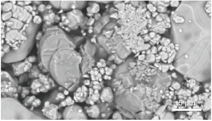
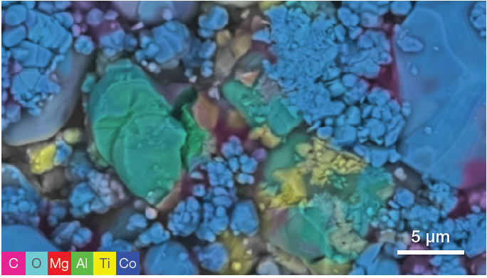
Figure 2. Traditional backscattered electron image (top) of the region of interest and quantitative elemental mapping (bottom) obtained with an acquisition of 80 seconds. (Acquisition parameters: acc voltage 10 keV, beam current 0.76 nA, dwell time 5 us). Image Credit: Thermo Fisher Scientific – Electron Microscopy Solutions
The characterization of one area of interest highlighted in Figure 1 is presented in Figure 2, further demonstrating this ability to focus on specific regions.
The backscattered electron image provided by traditional SEM imaging offers some initial feedback on the composition, but this does not offer sufficient information to successfully identify the contaminant.
The Axia ChemiSEM provides almost immediate access to quantitative elemental information each time a grayscale image is acquired due to the platform’s always-on X-ray detection.
These X-rays are acquired and processed in the background as part of the grayscale image acquisition, providing quantitative elemental information which complements the raw signal typically acquired via a conventional EDS gross counts mapping analysis.
This continuous access to elemental information equates to a seamless characterization experience – there is no need to wait for data; therefore, no time is wasted.
A quantitative elemental map (Figure 2) was collected in parallel with the conventional SEM image acquisition, with the user simply needing to activate the quantitative elemental view to access this.
Unlike a traditional EDS system, there was no need to re-acquire the data in this example.
A user can generate a complete set of images highlighting one element at a time (Figure 3) to achieve a better view of each element’s distribution.
The example presented here revealed the presence of Co - the main element from LiCoO2 – as well as Al, Mg and Ti within the electrode.
These latter three elements were unexpected contaminants that may have been introduced from the battery’s manufacture, for example, during the cathode materials’ synthesis, mixing or coating processes.
This approach means that the user remains focused on searching for odd, easily identifiable elements, leading to a more intuitive and accurate discovery process.
Point Analyses
Point analyses were executed to acquire the precise quantification of the elements present in the contamination. The example shown here focuses on Al.
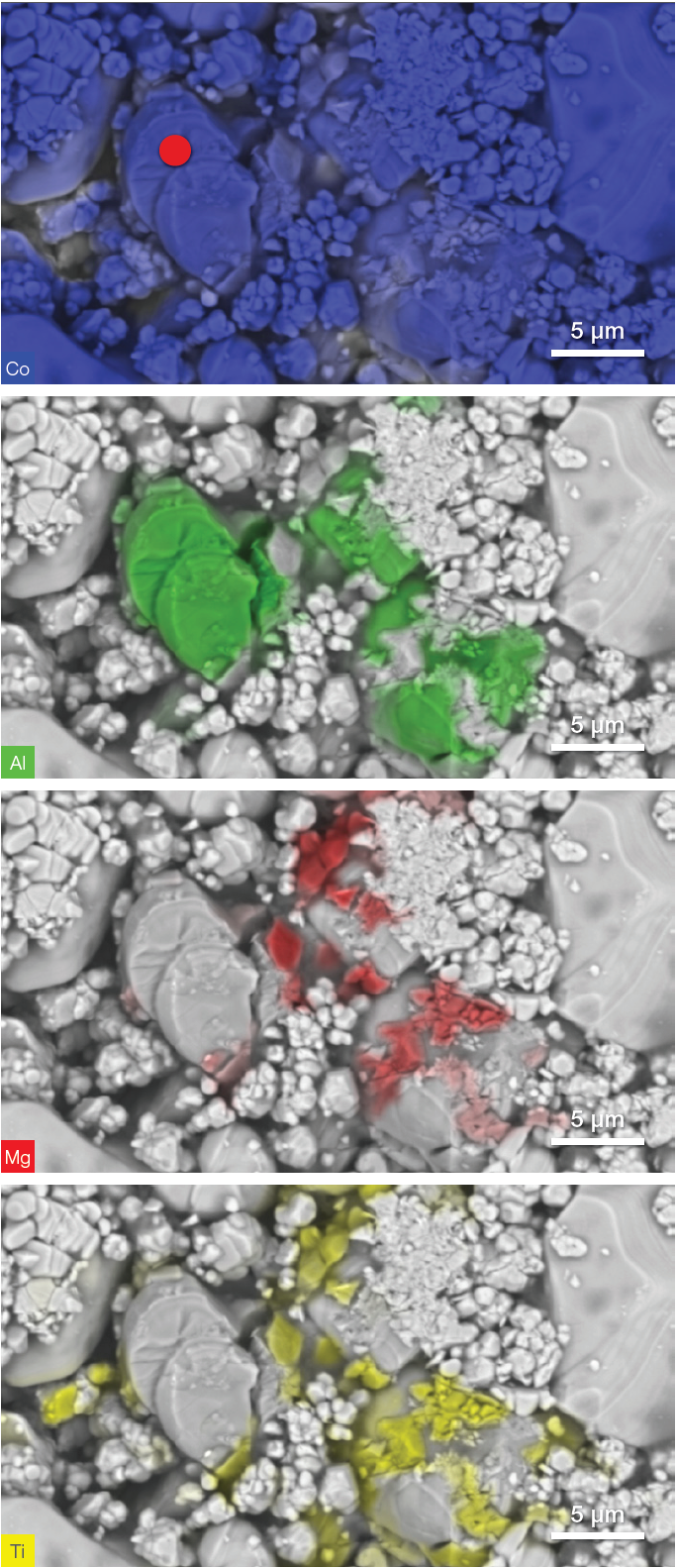
Figure 3. The first image on the top shows the distribution of the cobalt (Co) which is part of the battery matrix. The other three images highlight the distribution of aluminum (Al), magnesium (Mg) and titanium (Ti) contamination, respectively. The red dot in the top image shows the location where further analysis will be performed. Image Credit: Thermo Fisher Scientific – Electron Microscopy Solutions
The complete range of conventional EDS functionality is fully integrated into the Axia ChemiSEM user interface. This means that there is no need to switch to a different software package. The location of the point analyzed is illustrated by a red dot in the first image from the top of Figure 3.
Accelerating voltage and beam current have been reduced, and the same point analysis has been performed.
This allowed the exclusion of interaction volume effects on the quantitative results of the contaminant’s composition. Figure 4 shows a comparison of the analysis of that point as a function of acceleration voltage.
Axia ChemiSEM’s improved and intuitive graphical user interface offers automated system alignments, allowing changes in analysis parameters without manual adjustments and enabling rapid and straightforward analyses.
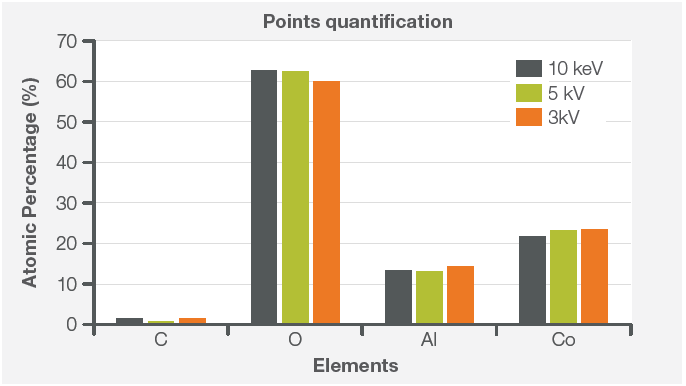
Figure 4. Contamination composition quantified at different acquisition conditions (10 keV and 0.76 nA, 5 keV and 0.28 nA, 3 keV and 0.16 nA). Image Credit: Thermo Fisher Scientific – Electron Microscopy Solutions
Point analyses were acquired using three different characterization conditions, lowering the accelerating voltage up to the minimum required to identify the contaminant’s composition and excite the Al k-line (1.4866 keV) (Figure 4). Results were comparable, irrespective of accelerating voltage.
The contaminant’s composition remained consistent, confirming that an amount of Al is embedded in the LiCoO2. This suggests that Al reacted with the precursor used to synthesize LiCoO2 during the sintering process.
These results would allow a researcher to conclude that it is necessary to carefully examine the raw materials for LiCoO2 synthesis or the equipment involved in the sintering process to eliminate this contaminant.
Conclusion
A comprehensive assessment of contaminants within battery materials is a core factor in assuring battery quality and performance.
The Thermo Scientific Axia ChemiSEM offers robust large-scale SEM-EDS mapping, and this was used in the example presented here to quickly and easily identify contaminants.
It was then possible to seamlessly move into detailed quantitative EDS analysis to determine the distribution of each contaminant more precisely.
Point analyses were performed to confirm the precise quantification of each element found in the contamination.
Use of the Axia ChemiSEM means no longer working with SEM imaging and EDS as separate workflows – these are now components of an integrated process designed to rapidly move from discovery to analysis to generate accurate results with ease.
The combination of live EDS technology and the Axia ChemiSEM’s automatic alignment function affords users a smooth experience and enables the efficient characterization of the battery electrode.
By leveraging the power and efficiency of the Axia ChemiSEM, battery manufacturers can perform rapid and straightforward SEM-EDS contaminant analysis, improving the efficiency of their research, reducing contaminants during the manufacturing process and enhancing battery performance.

This information has been sourced, reviewed and adapted from materials provided by Thermo Fisher Scientific – Electron Microscopy Solutions.
For more information on this source, please visit Thermo Fisher Scientific – Electron Microscopy Solutions.