It has been over 30 years since the first focused ion beam was used to make a TEM specimen. FEI, a company that is now part of Thermo Fisher Scientific, has been an essential part of helping take ion beam technology to where it is today. Thermo Fisher Scientific offers users the ability to use not only gallium ions but a variety of focused ion beams made with noble species like Xenon or Argon.
We spoke with staff scientist for application development, Dr. Chengge Jiao of Thermo Fisher Scientific, about the use of a focused ion beam without gallium to move toward damage-free TEM specimen preparation.
In this interview, Thermo Fisher Scientific explores the rewards of using a focused ion beam without gallium for sample preparation and whether a damage-free sample can be predicted.
Please could you introduce yourself and outline your role at Thermo Fisher Scientific?
I am Dr. Chengge Jiao, a staff scientist for application development. I have been part of FEI - now Thermo Fisher Scientific - for more than 20 years. My particular experience is in both focused ion beams and a range of analytical techniques for material science applications.
What is gallium-free TEM specimen preparation by a focused ion beam (FIB)? Is gallium-free preparation sufficient for a TEM specimen to be “damage-free”?
What most TEM microscopists think of when you say Focused Ion Beam (FIB) is the gallium ion beam. The gallium and the specimen’s ion beam damage have always been the major concerns for the quality of a TEM specimen. Gallium-free TEM specimen preparation is about using a FIB other than Ga+ for TEM specimen preparation.
For FIB gallium TEM specimen preparation, the gallium is not only implanted in the solid but also has an affinity with some materials, such as with aluminum atoms, for example, at the interface between a single-crystal aluminum thin film on a silicon substrate; this makes the aluminum atoms show as a contrasting strong white at the interface. A Plasma FIB Xenon ion beam prepared specimen is gallium-free. The interface HAADF STEM contrast is most likely related to the interface strain effect.
What we have learned from the case of TEM specimen preparation from aluminum alloys is that one of the advantages of plasma Xenon FIB for TEM specimen preparation is avoiding affinity or even alloying between injected ions and target atoms, especially at the interfaces and grain boundaries. This is because of the inertness or inactiveness of Xenon.
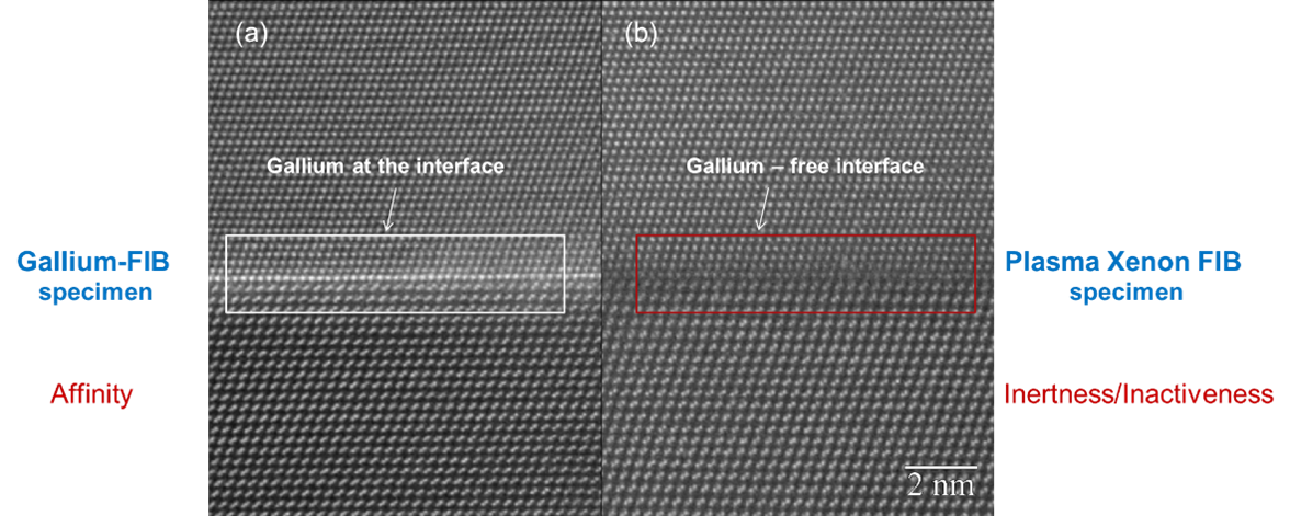
Aluminum/Silicon interface: Al thin-film deposited on Si. Titan 80 – 300 STEM HAADF Z-contrast, (a) Gallium FIB, (b) PFIB Xenon prepared specimen. Sample preparation credit: Thermo Fisher Scientific. Image credit: Thermo Fisher Scientific
Gallium-free does not equal a “damage-free” TEM specimen.
To achieve a “damage-free” TEM specimen, a proper FIB ion species needs to be used. Therefore, we need to answer questions such as, what are the benefits of using focused ions other than gallium apart from the specimen being free of gallium ion implantation? Can we get a “damage-free” TEM specimen by focused ion beam (FIB)? Can we predict the damage of argon, gallium, xenon ions to the sample?
What is a “damage-free” TEM specimen?
A TEM specimen requires an order of magnitude less damage in contrast to an EBSD sample. Less than 5 nm thick damage is essential for a high-quality, less-damaged TEM specimen. To achieve a “Damage-free” specimen, the damage layer needs to be less than 1 nm thick.
This graph defines FIB sample preparation application domains, such as beam performance, less damage, and so-called “damage-free.”
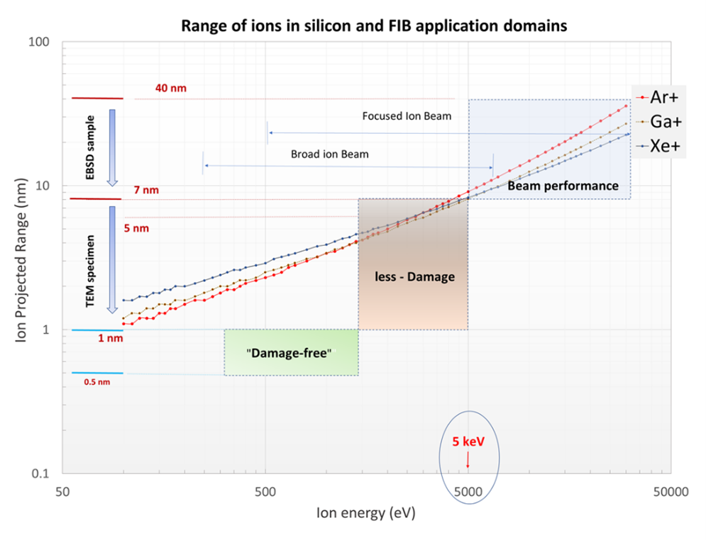
Image credit: Thermo Fisher Scientific
In terms of microscope operation, we can separate it by a high keV and a low keV.
The domain is classified based on the ion’s projected range in silicon of argon, gallium and xenon ion species as a function of the ion energy from 100 eV to 30 keV.
It shows that for the same ion, the lower the ion energy, the shorter the ion’s projected range. We will discuss different ions in more detail later.
High keV normally refers to beam energy above 5 keV as high energy, and most FIB users use it at 30 keV. The major concern is beam spot size, shape, and profile for milling and imaging.
Low keV ion energy is below 5 keV, aiming for less damage or “damage-free” sample preparation for EBSD and TEM specimens.
What can be done to move towards damage-free TEM specimen preparation?
You need to consider at least three things for FIB “damage-free” sample preparation:
- Reduce the FIB energy below 1 -1.5 keV for sample preparation - A multi-ion source Helios Hydra plasma FIB argon ion beam can be operated as low as 500 V.
- Select a proper type of ion for the sample preparation.
- Apart from damage thickness or range, it is important to consider the host atom displacement intensity induced by the incident ion.
Why is it important to understand the atom displacement vacancy?
To evaluate sample damage by an ion beam, we need to understand the target material damage caused by energetic particles first.
Beam damage includes knock-on damage and beam-induced heating dominantly caused by photons which are predominantly created by the recoil.
In this presentation, we are concerned about knock-on damage. They are Displacement, Vacancy, Interstitial atoms and Replacement collisions.
To prepare a “damage-free” TEM specimen, we need to consider not only the ion range but also the atom damage intensity induced by the ion.
As an incident ion slows down by nuclear and electronic stopping and comes to rest, the ion collides with the lattice atoms, displacing them from their lattice sites, and the displaced atoms can, in turn, displace others. Thus, a track of the target atom lattice-disorder region around the ion path is formed.
The disordered track can be observed by TEM in the form of point and cluster defects and also dislocation loops, assuming that no recovery of lattice order occurs around the ion track.
An amorphous layer is formed by accumulated damage in overlapped, highly disordered regions where the defect density is above the critical point defect density threshold.
The ion range is related to the amorphous layer thickness, and the damage intensity is related to obtaining a “damage-free” specimen. To achieve a “damage-free” TEM specimen, a sample preparation process with both low ion range and low damage intensity is required.
What can be seen in the analysis of the simulated ion range at 30 keV energy, and specifically the analysis of the vacancy per ion?
We cannot find a suitable ion species giving both low ion range and low damage intensity at 30 keV.
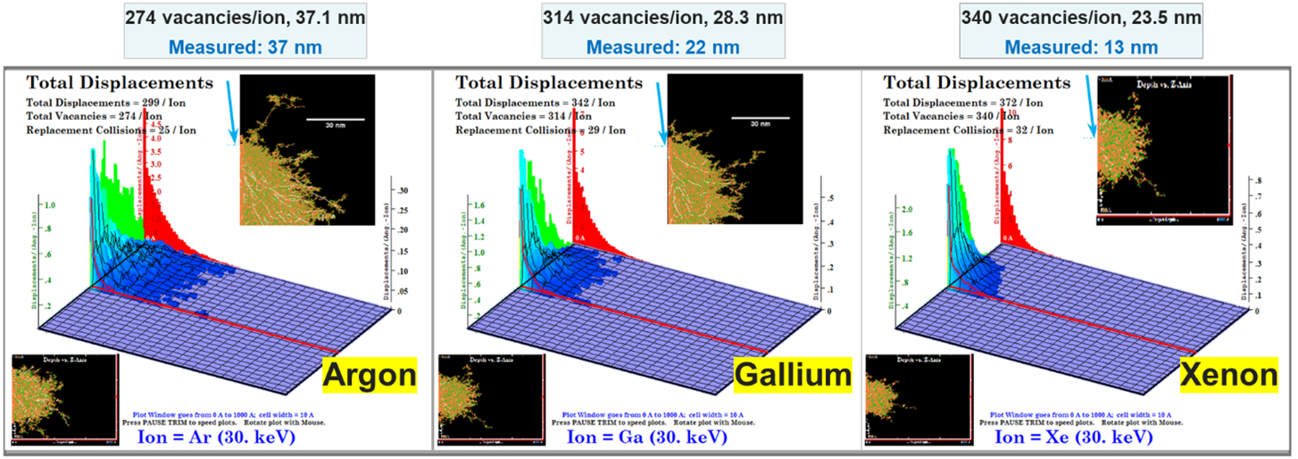
Image credit: Thermo Fisher Scientific
The argon ion range has a large spread, but it has a smaller vacancy per ion generated. It is thus clear that the xenon is opposite to the argon. The problem is that at 30 keV, there are no ion species provided by FIB that have both a low ion range and low damage intensity.
Xenon is the most suitable choice for 30 keV applications because the ion range is low. If the range is low, that potentially means that the amorphous layer thickness is lower. If xenon is used for other applications - for example, for SIMS depth profiling - the depth resolution will be better than other ion species.
If we make a TEM specimen 100 nm thick at 30 keV energy, how much of the thickness will be “damage-free”?
To answer this question, the ion can be positioned at an 88 degree angle from the 100-nanometer thick specimen, shooting into the front and the back of the specimen so that the ion incident angle is two degrees. A 50-nanometer marker is then placed.
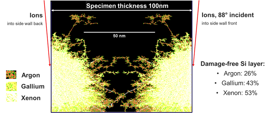
Ions (Ar+, Ga+, Xe+) distribution and silicon atom recoil projected on Y-plane from the front and the backside of 100 nm thick TEM specimen. Image credit: Thermo Fisher Scientific
Ions of argon, gallium or xenon distributions and silicon atom recoils were superimposed for a visualization, ions at 88° incident to silicon on the front and the back sidewalls, with the specimen at 100 nm thick.
The brightest and also smallest area is xenon, compared to the wider spread argon ions and silicon atom recoils.
You can see the argon-prepared specimen contained a damage-free zone that is only about 26 nm thick (or 26%) in a 100 nm thick specimen. The Xenon ion beam at 30 keV produces the specimen with the largest portion of non-damage.
The takeaway messages are that xenon should be used at 30 keV and that a TEM specimen below 50 nm thick prepared at 30 keV by any type of ions will end with a fully damaged specimen.
Why is a sputtering yield necessary for analysis in this instance?
It is important to work on a sputtering yield. A ”damage-free” TEM specimen will not benefit from an ion species that provides a high sputtering yield. A high sputter yield means:
- High secondary recoils
- More collisions near the surface
- Large atom displacement (high damage density)
- Low ion implantation.
Sputtering yield depends on the incident angle, target material, the type of ion species, and the ion beam.
Xenon at 30 keV has a high sputtering yield. However, at 30 keV, argon’s sputtering yield is only half that of xenon. This means that if you have a high sputtering yield, you will get a target host atom with high second recoil. The high second recoil, therefore, gives a large item displacement – and potentially, a higher damage intensity. A high sputtering yield also means that there is potentially a far more uneven surface generated by the sputtering.
An advantage, therefore, appears if a xenon beam is used at 30 keV as a faster sputtering yield will be achieved. Thus, users tend to prefer using a xenon beam for large volume material removal. The preference can be attributed to both the high current and high sputtering yield. If the argon beam is chosen, this can result in a much smoother surface. This lower sputtering yield offers a gentle beam for low keV cleaning and makes a low keV process easy to control.
Could you reference an example to illustrate the advantage of different ion species for 30 keV or lower keVs applications?
Let us consider a graphite layer on an electrode. The graphite layer cross-section prepared by Xe+ beam at 30 keV has curtains. However, on the 30 keV argon-prepared specimen, the cross-section is very smooth. That tells us that the argon has an application at 30 keV. Although using an argon beam at 30 keV to prepare TEM specimens to a thickness below 500 nm is not recommended.
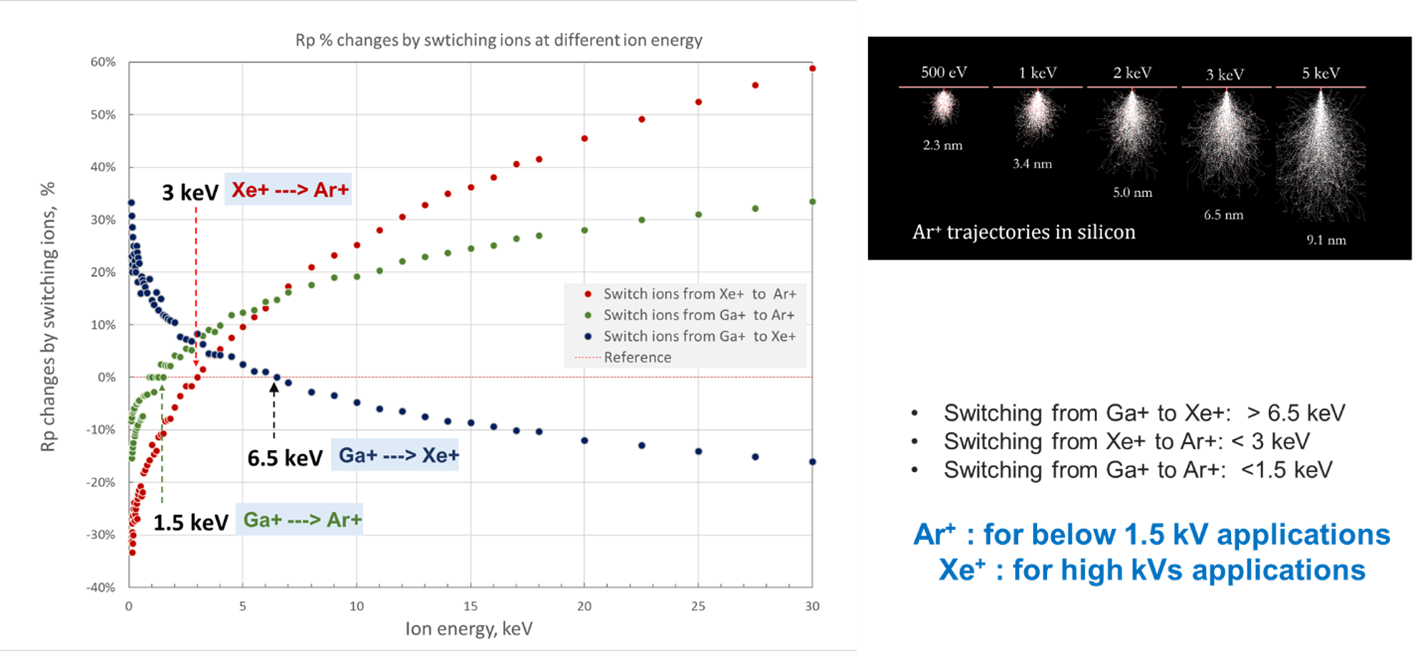
Image credit: Thermo Fisher Scientific
Let us consider low keVs and examine the beam at a normal instant. Analysis can be commenced by switching ions to the three different ‘switching points’ between the gallium, xenon, and argon. ‘Switching points’ means the ion’s projected range change becomes a negative change.
When the beam energy moves over 6.5 keV, it is always a negative change in the projected range. That means when the beam energy is more than 6.5 keV, it is better to use a xenon ion beam for applications.
However, below 1.5 keV, the argon ion beam is the best. This, therefore, means that argon can be used with a normal incident to prepare an EBSD sample. For example, we have used Ar+ at 500 eV to clean a very sensitive aluminum-lithium alloy surface for UHR SEM images of nanoparticles by a monochromated SEM.
If we consider a shallow incident angle with ion energy from 5 keV to 300 eV, the argon-generated damage density is lower than gallium and xenon. The gallium measurement is between xenon and argon.
When the ion energy drops below 1.5 keV, the argon starts to give a lower ion range on the XZ plane - which is related to the TEM specimen thickness. Therefore, argon can gain both a lower damage density and a lower ion spread into the material. Argon ions at low energy are a good choice for “damage-free” TEM specimen preparation.
Let’s look at Talos microprobe TEM images at 200 kV acquired by a Ceta 16M camera from FIB prepared TEM AlGaN/GaN TEM specimens.
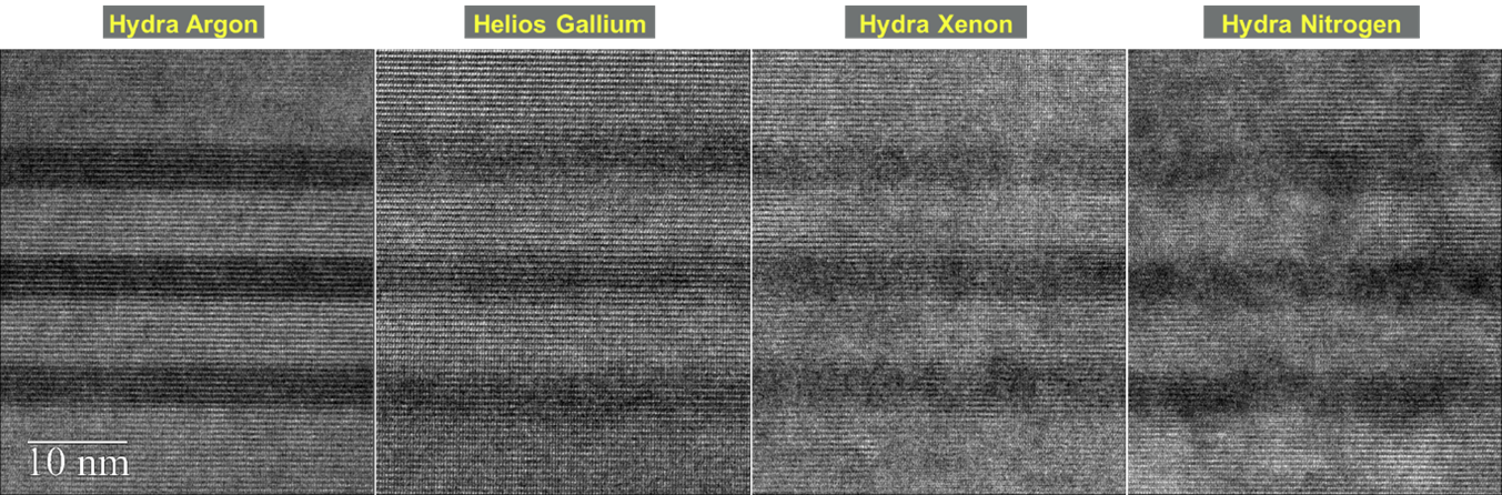
Image credit: Thermo Fisher Scientific
The sample is epitaxial layers AlGaN/GaN, and specimens were thinned gradually by reducing ion energy from 30 keV to 8 keV -> 5 keV -> 1keV with different ions.
Clearly, the argon ion beam prepared TEM specimen is the winner.
- The argon ion beam prepared TEM specimen brought a clean and clear interface between AlGaN/GaN/AlGaN. This because it causes less damage and has fewer chemical reactions between the incoming ion and the host atoms.
- The xenon ion beam prepared specimen is good with very little changes in the AlGaN layer, showing that it benefited from a gallium-free TEM specimen preparation process.
- The gallium ion beam prepared specimen also looked good, however, the AlGaN layer has been modified and the interface is not well defined. This perhaps is caused by chemically reactions between gallium and AlGaN.
In terms of atomic radius, the argon is the smallest among argon, gallium and xenon.
If we use an even smaller atom, like a nitrogen ion for specimen preparation, what will happen?
Therefore, here, a TEM image prepared by nitrogen ion is also presented. What you can see there are clusters of strong, dark contrast in the TEM Microprobe image (parallel beam not in STEM mode). We believe the black clusters of contrast might be caused by a reaction between nitrogen with GaN and AlGaN, thus likely forming nitrides locally. If we zoom in and look at the non-cluster areas, we can see the TEM image in the non-dark area is very good, as it perhaps benefited from the small atomic radius of the nitrogen ion.
By the way, the final thickness of the specimen is less than 40 nm.
What can be seen in the analysis of the vacancy distribution from 1 keV to 500 keV?
We focused on data generated from ions at an energy of 1 keV and 500 eV. The damage intensity by argon was the lowest. Xenon’s damage intensity was about 2.44 times greater than argon’s, and gallium’s damage intensity was about 1.9 times greater than argon’s.
For a 500 eV argon final polished TEM specimen of a metal and metal-oxide interface, the specimen was thinned by reducing the accelerating voltage from 5 kV - 2 kV – 1 kV and was finally “washed” by 500 eV energy argon ion beam using a Helios Hydra multi-ion source Plasma FIB DualBeam.
You can see the overview of the specimen from a 200 kV Talos STEM BF image.
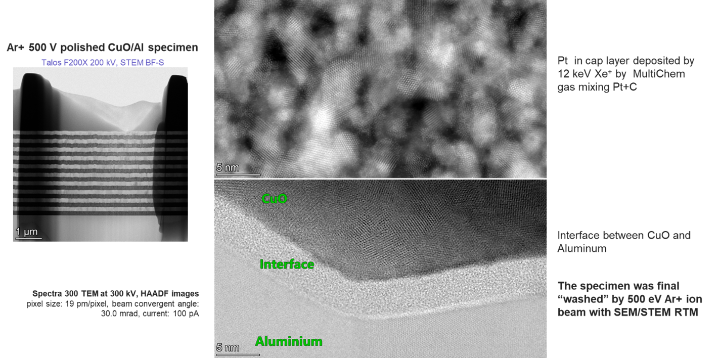
Image credit: Thermo Fisher Scientific
Atomic resolution STEM HAADF images acquired by 300 kV Spectra TEM are displayed on the right. You can see a clear interface between the CuO and aluminium layers, it also shows platinum lattice images in the cap layer. By the way, cap layer deposition is very important for plasma FIB TEM specimen preparation, the cap layer was deposited by platinum and carbon gas mixing delivered by MultiChem GIS under a 12 kV Xenon ion beam.
In conclusion, we are close to a ‘damage-free’ TEM specimen preparation process through the introduction of a high-performance, low-energy focused argon ion beam in our FIB.
What are the key takeaways from your presentation?
The key takeaways from this are that a Xe+ prepared TEM specimen is “clean” compared with Ga+ because xenon is inert without inducing ions-atoms chemical reactions; this is the so-called “Gallium-free”. Both ion range and target material atom displacements are important for making a damage-free TEM specimen.
Xenon ion has the lowest ion range compared with argon and gallium ions. It is thus recommended to choose xenon ions for 30 kV applications. In terms of ion-induced damage intensity or induced defect density (vacancy per ion per nanometer) for FIB TEM specimen preparation, Xe+ > Ga+ >Ar+, so xenon ions are not good enough to produce a “damage-free” TEM specimen.
From the ion range and damage intensity points of view, the Gallium-FIB (G-FIB) DualBeam prepared specimen is better than the xenon ion beam in the case where gallium contamination to the specimen can be tolerated. Argon below 1.5 keV is the best choice for a “damage-free” TEM specimen.
Zero damage sample preparation is very challenging and often even not possible, but with the latest innovations in multiple ion species plasma FIB technology, high-quality results can be achieved. Predicted data shows that a specimen is around 85% damage free (25.5 nm) within a 30 nm final thickness by Ar+ ion beam at 300 V. If the Ar+ is at 500 eV energy, the damage-free layer is about 83% (25 nm) in a 30 nm thick specimen.
About Dr. Jiao
Chengge Jiao is a staff scientist for application development in Thermo Fisher Scientific in Eindhoven, the Netherlands. He joined the company in the UK as a FIB application engineer about 20 years ago after a post-doctoral researcher position in the school of physics, university Bristol, UK where he worked on electron holography of GaN materials by a cold-FEG TEM. He is an experienced electron microscopist with knowledge of materials science. His current interest is to apply multi-ions species (Xe+, O+, Ar+, N+) Plasma Focused Ion Beam (MIS-PFIB) and FIB-SIMS for material science applications. Chengge received his PhD in materials science from the University of Birmingham, UK on an investigation of dislocation microstructures in MoSi2 intermetallic by TEM. He has authored or co-authored over 50 publications including in Physical Review Letters (PRL), Nature Materials, Acta Materialia.

This information has been sourced, reviewed and adapted from materials provided by Thermo Fisher Scientific – Materials & Structural Analysis.
For more information on this source, please visit Thermo Fisher Scientific – Materials & Structural Analysis.
Disclaimer: The views expressed here are those of the interviewee and do not necessarily represent the views of AZoM.com Limited (T/A) AZoNetwork, the owner and operator of this website. This disclaimer forms part of the Terms and Conditions of use of this website.