Piezoresponse force microscopy (PFM) is an effective method for examining ferroelectric materials due to its nanometer-level resolution and high sensitivity, inherited from atomic force microscopy (AFM).
PFM-based spectroscopic techniques, such as switching spectroscopy PFM (SS-PFM) and DataCube™ PFM (DCUBE PFM), enable the characterization of essential parameters of ferroelectrics, including nucleation voltages, coercive voltages, and saturation responses.
Unfortunately, artifacts may complicate quantification and subsequent interpretation of PFM results. The best methods and practices for optimizing PFM measurements to enable reliable results are discussed below.
There are many variations to the PFM technique that can be used to examine various aspects of electromechanical response (as shown in Table 1). This article centers on the recently developed SS-PFM and DCUBE PFM modes and how they may be able to help with numerous issues.
The advantages of resonance and sub-resonance PFM are considered alongside optimizing laser position to enhance measurement accuracy.
Table 1. AFM modes and methods for PFM. Source: Bruker Nano Surfaces
| PFM Mode/Method |
Benefits |
| Sub-resonance PFM with laser at electrostatic blind spot |
Eliminates electrostatics, simple calibration |
| Sub-resonance PFM with laser at tip |
No need to position laser at ESBS, simple calibration |
| Contact Resonance PFM |
Significant PFM signal amplification, but must consider CR shape factor for quantitative measurements |
| Contact Mode PFM |
Fast and simple especially for sub-resonance PFM |
| DCUBE PFM mapping |
Minimizes tip wear and sample damage, simultaneous mapping of PFM response and mechanical properties such as modulus & adhesion, works with either contact resonance or sub-resonance PFM |
| SS-PFM spectroscopy and mapping |
Same as DCUBE, but additionally allows separation of read and write segments, and use of multiple read segments at different voltages for cKPFM and PFM spectroscopy |
| Vector PFM (vertical and lateral) |
Characterize different components of piezoelectric response tensor |
| High Voltage PFM |
Switch samples with high coercive voltages and/or measure low-response samples |
| PFM Lithography |
Control ferroelectric domain structure and/or investigate domain wall propagation |
Background
To study the electromechanical response of materials using PFM, a sinusoidal (AC) drive voltage is employed between the sample substrate and a conductive AFM probe. The inverse piezoelectric effect triggers the sample to expand and contract sinusoidally; an AFM probe tip contacting the sample surface can identify this.
Materials with a positive electrostrictive coefficient, for example lead zirconate titanate (PZT), expand when the polarization of a piezoelectric domain below the tip is parallel to a growing electric field, and vice versa.
The AFM tip is displaced, and the cantilever bends when the sample expands, generating a sinusoidal signal in deflection at a frequency identical to the AC drive voltage (as shown in Figure 1a).
It is noteworthy that certain piezoelectric materials, e.g., polyvinylidene difluoride (PVDF), have negative electrostrictive coefficients.
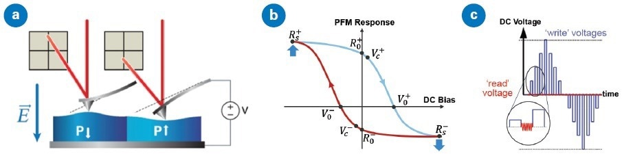
Figure 1. Piezoresponse Force Microscopy (PFM) basics: (a) an increasing electric field in parallel with the polarization of a piezoelectric sample will cause the sample to expand if the material has a positive electrostrictive coefficient, (b) a typical hysteresis loop describing the response and domain switching characteristics of a ferroelectric material, and (c) a series of read and write pulses applied during switching spectroscopy PFM (SS-PFM). The write segments use successively larger (or smaller) DC voltages to switch the polarity of the domain beneath the tip, while an AC voltage is applied during read segments allow observation of the polarization and response of the domain after switching. Image Credit: Bruker Nano Surfaces
Due to the ability of AFM to measure deflection parallel to the sample surface (perpendicular to the cantilever), it is possible to measure two orthogonal components of the piezoelectric displacement vector simultaneously.
Rotation of the sample by 90° can offer the third component, enabling full characterization of the displacement vector.1
If the material is ferroelectric, applying a substantial enough voltage (namely, the coercive bias) has the ability to cause the domain polarization to flip. This new polarization is subsequently retained after the removal of the voltage.
Figure 1b presents a standard ferroelectric hysteresis loop for a material with a positive electrostrictive coefficient, such as PZT. Key parameters in the loop include nucleation voltages (Vc±), coercive voltages (V0±), saturation responses (RS±), and remnant responses (R0±).
The goal of PFM spectroscopy is the local measurement of these hysteresis loops and their associated parameters.2
Switching spectroscopy PFM (SS-PFM) advances the accuracy of PFM spectroscopy by differentiating measurements of the PFM response during write voltages from those during read voltages (see Figure 1c).3
The AC voltage is removed during a write segment and then resupplied during a read segment to examine the domain stability after poling.
Quantitative PFM allows the validation of results utilizing different probes and labs. However, there are challenges and difficulties associated with conducting quality PFM measurements:
- Signal levels are frequently quite small (<10 pm/V), causing difficult detection.
- PFM is sensitive to many distinct types of electromechanical responses of the sample, which may be complicated to separate.4
- The detected signal is affected by the measurement system (AFM and probe) as well as the sample. An example of this is how electrostatic forces between the cantilever and surface or background signals from within the AFM may cause a response comparable to that of a piezoelectric material.5
- PFM results may lack consistency if the tip or sample is impaired by the uncontrolled lateral forces that take place during contact mode scanning (the conventional mode for PFM scanning).
Maximizing Sensitivity
Generally, the signal levels in PFM are minute, with usual amplitudes <10 pm/V. This is nearing the limit of what an AFM is able to detect. To deal with this, one of the four following approaches is usually taken:
1. Increasing the AC stimulation voltage:
Due to the PFM amplitude being proportional to the AC stimulation voltage (to a first order approximation), doubling the AC voltage approximately doubles the PFM response. Arbitrarily increasing the AC stimulation voltage, however, is not a typically useful approach.
Numerous samples hold weak points where current leaks, causing dielectric breakdown and sample harm at high voltages. In addition, ferroelectric sample domains flip (pole) if the AC voltage exceeds the coercive voltage.
This results in the measured amplitude no longer reflecting a purely piezoelectric response and the hysteresis loop beginning to collapse. The nucleation voltage is often <5 V for thin films, substantially restricting the practical AC amplitude.
2. Increasing the amplification of the deflection signal:
Another approach to enhancing PFM signal levels is to increase the amplification. Amplification removes bit-noise, but the signal-to-noise ratio (SNR) is only marginally improved.
Signal amplification (by a factor of 16) is offered to all Dimension Icon® users by selecting the “Optimized Vertical” or “Vx16” workspace.
3. Increasing the time constant of the lock-in amplifier:
Increasing the time constant of the lock-in amplifier results in increasing averaging, which decreases noise. This reduction in noise is at the cost of update time, causing slower data acquisition, but it is worth being considered for low-response samples.
4. Amplifying the PFM motion mechanically:
PFM vibration may be amplified mechanically utilizing the cantilever contact resonance. This technique, contact resonance PFM (CR-PFM), provides a substantial (up to 100x) increase to PFM sensitivity. This permits amplitudes detection as low as <1 pm, but it does also increase complexity.
Quantifying CR-PFM amplitude necessitates calculation of the CR shape factor from the contact resonance amplitude, frequency, and quality factor (Q).6
CR-PFM measurements may be obtained at a set frequency or with the use of a resonance tracking technique, such as dual-frequency resonance tracking (DFRT), frequency sweeps, or band excitation (BE).
The CR frequency typically changes during scanning, and as a result, fixed-frequency measurements near resonance are not advised for quantitative PFM.
It is preferable to utilize Ramp, RampScript, or force volume-based (FV-based) techniques that have the ability to accurately control the forces while detailed frequency spectra are collected.
Improving Repeatability with DataCube Methods
DataCube (DCUBE) CR-PFM is an FV-based hyperspectral imaging method that delivers maps of CR-PFM amplitude with related Q factor, frequency, and phase on resonance. Figure 2 displays an example of DCUBE CR-PFM results obtained from a PMN-PT sample to show how the method works:
- A force curve is collected with a surface hold segment (see Figure 2a) at each pixel in the image.
- The frequency of the AC stimulation voltage is swept over a user-specified range while deflection amplitude and phase spectra are collected (see Figures 2b and 2c, respectively), during the hold segment.
- Analysis of spectra takes place and results are utilized to produce maps of sample properties over the scan area (see Figures 2d-f).
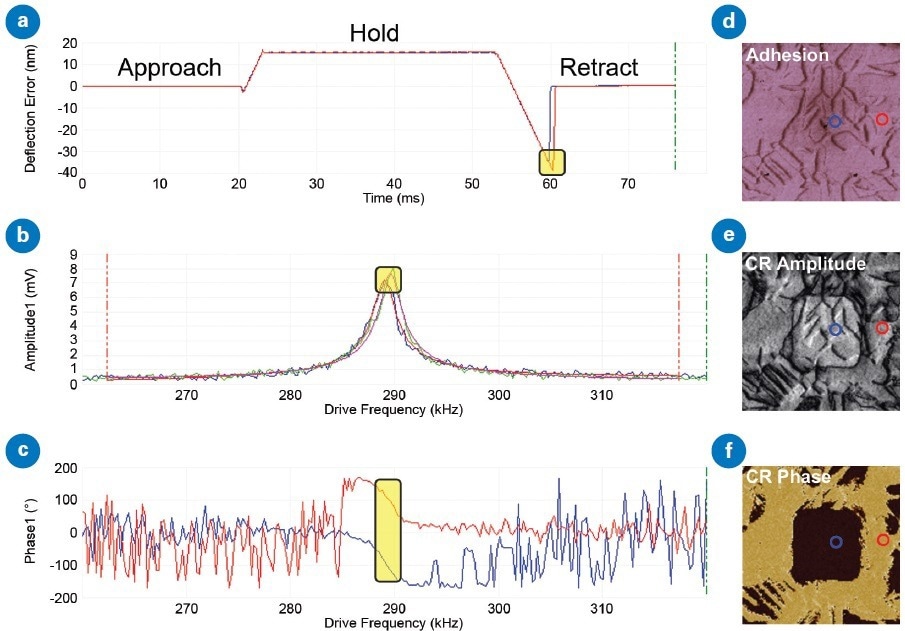
Figure 2. DataCube (DCUBE) CR-PFM of a PMN-PT ferroelectric sample: (a) Typical force vs. time plots showing 30 ms hold segments where frequency is swept and highlighted pull-off points for adhesion map, (b) PFM Amplitude spectra from hold segment and Lorentzian fits used to calculate CR Amplitude (peaks highlighted), Frequency, and Q, (c) PFM Phase spectra used to determine CR Phase (region of CR highlighted), (d) Adhesion map with approximate locations of curves in (a), (e) CR Amplitude map with locations of curves in (b), and (f) CR Phase map with locations of curves in (c). Image Credit: Bruker Nano Surfaces
The typical force curve approach and retract data is accessible along with the hold segment, enabling the usual fitting and obtaining of maps of mechanical properties, such as modulus and adhesion (see Figure 2d), from the same dataset.
Due to the sweep width, duration, and sampling rate of the hold segment being controlled by the user, the CR-PFM maps may be optimized for SNR and accuracy. Figure 2b displays how two standard CR-PFM spectra are fit to produce maps of CR Amplitude (see Figure 2e).
Once the exact CR frequency is determined, the CR Phase may be obtained (see Figure 2c) and the related map produced (see Figure 2f). The contact resonance frequency, Q, and amplitude are specified by fitting hundreds of points, enabling increased accuracy over dual-frequency resonance tracking (DFRT)-based methods – particularly for Q.
When long hold times are accepted, long integration times (increased lock-in time constants) are feasible. If there are several CR eigenmodes of interest, these may be collected in a single pass by increasing the frequency sweep width; some care is necessary to prevent distortion of the resonance peaks from sweeping too rapidly.
Since DCUBE techniques are based on FV, the tip does not drag on the surface between measurements, eliminating the lateral force that happens in contact mode and which frequently damages probes and samples. The tip apex is protected, causing measurements that are more consistent than similar contact mode techniques.
DCUBE allows measurements on samples that are prone to damage or displacement by dragging the AFM tip on the surface, such as fibers and nanoribbons. Softer cantilevers are able to partly alleviate this issue, but are more susceptible to electrostatic artifacts than stiffer cantilevers.
Phase Considerations
For PFM results to be reliable, it is essential to counteract any instrument-induced phase shift. Digital lock-ins have a fixed time delay for data processing. As the rate increases, this fixed time delay causes an approximately linear increasing phase shift.
Due to the shift varying comparatively slowly with frequency (see Figure 3a: ~0.4°/kHz), a straightforward subtraction of an offset phase is usually adequate to compensate for the issue.7 When using the same type of probe, the required offset phase will be comparable since the cantilever resonance frequencies are similar.
However, any variation in the signaling path, including microscope cable length, can alter the phase shift. A lack of compensation of the instrumental phase shift can cause an inversion of the PFM hysteresis loops (see Figure 3c).
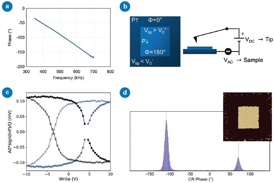
Figure 3. Compensating for instrumental phase shifts: (a) the measured phase from the lock-in depends approximately linearly on frequency, with a phase shift of about -4 deg/kHz, (b) domain polarization and expected phase after applying negative and positive DC tip voltages to pole concentric domains in a ferroelectric sample with known positive electrostrictive coefficient, (c) if this phase shift is not compensated, the direction of ferroelectric hysteresis loops may be inverted when probes of different frequencies are used, and (d) histogram of phase data from a DCUBE CR-PFM map (inset) after poling with pattern in (b) has peaks at -109° (outer domain) and +71°. Image Credit: Bruker Nano Surfaces
To establish the phase shift at any particular frequency, the method of Neumayer et al. is followed,7 utilizing a reference ferroelectric sample to initially produce and then measure domains of known orientation.
Materials such as PZT and PMN-PT are understood to have positive electrostrictive coefficients. An increasing electric field employed in parallel to the polarization of a domain in the material will cause an expansion of the material.
The application of a large enough negative voltage to the tip (electric field up) makes it possible to flip the domain polarization up and then pole and measure two concentric squares (see Figure 3b):
- Negative DC voltage (<V0-) to the tip for the outer square
- Positive DC voltage (>V0+) to the tip for the inner square
- Set DC voltage to zero and scan the area to measure the PFM phase
When the sample has AC voltage applied, the phase of the outer square should be 0° (inner at 180°). Since the lock-in phase range is ±180°, the inner domain tends to wrap (noise triggering the phase to switch between +180° and -180°).
It is preferable to avoid this wrapping by adjusting a lock-in parameter (the drive phase) to make the outer domain +90° (inner at -90°). If this occurs, the -90° should be added back to the data when it is analyzed.
Figure 3d shows a Bruker SCM-PIT-V2 probe utilized with free resonance frequency 62.7 kHz (CR frequency 282 kHz). The outer domain exhibited a mean value of -109° (with lock-in drive phase of 0°), and the following data was gathered with a lock-in drive phase of +90° + 109° -0° = -161°.
The resulting hysteresis loops exhibit a clockwise direction, as expected.
Electrostatic Signal
A key challenge for researchers seeking to quantify their PFM measurements is the effect of electrostatic forces from the sample impacting the full length of the cantilever (see Figure 4a).
The electrostatic signal is proportionate to the contact potential difference (CPD) between sample and tip, and linearly adds to the material’s piezoelectric response.
When the CPD is changed by the charge injection from the tip, this can cause non-ferroelectric materials to exhibit a PFM response that is comparable to that of ferroelectric, even displaying the typical hysteresis loops and butterfly amplitude loops.5
To begin to understand and dissociate this electrostatic signal from the piezoelectric signal, at least one of several approaches is commonly used, each with its own advantages and disadvantages, as discussed below.
Increasing cantilever stiffness
With identical electrostatic force, stiffer cantilevers bend less, resulting in a smaller impact from the electrostatic signal (contrastingly, the piezoelectric response is insensitive to the cantilever stiffness, with the exception of very soft samples).
Recently, this was confirmed for sub-resonance PFM, where the electrostatic contribution was lower than the piezoelectric contribution for spring constant (kc) over approximately 25 N/m on periodically poled lithium niobate (PPLN).8
Sample damage and tip wear may arise with very stiff probes in contact mode. Cantilevers that are softer than kc=10 N/m are generally preferred for PFM measurements on stiff samples (with the exception of low-resolution).
However, with SS-PFM and DCUBE PFM, the uncontrolled lateral forces that take place during contact mode are averted, allowing the utilization of relatively stiff probes with minimal harm to the tip or sample.
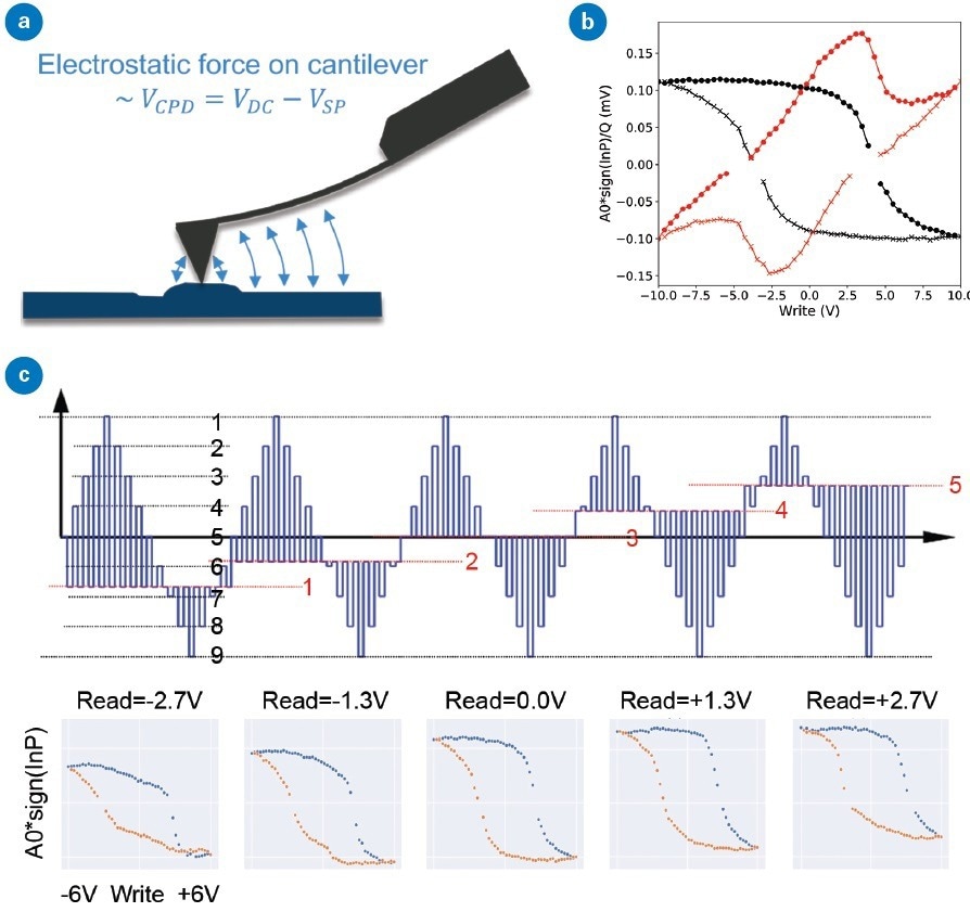
Figure 4. Understanding the influence of electrostatics on the PFM response: (a) the electrostatic force on the cantilever is proportional to the contact potential difference or the difference between the applied voltage (VDC) and the surface potential (VSP), (b) comparing PFM hysteresis loops collected during read segments (black) and write segments (red) can be used to discriminate between ferroelectric and non-ferroelectric materials, and (c) by measuring SS-PFM hysteresis loops (bottom) at different read voltages (top) it is possible to directly study the influence of varying contact potential difference on PFM measurements. Image Credit: Bruker Nano Surfaces
Using SS-PFM to investigate bias dependence
An alternative approach is the application of a DC bias during SS-PFM spectroscopy to examine changes in electrostatic forces that arise following charge injection. Bruker’s SS-PFM implementation enables this to be carried out in two distinct ways: 5
- Comparison of the hysteresis loops with measurements that were obtained during the write segments (at a range of voltages) with those obtained during the read segments (at zero bias).
- Successively taking the SS-PFM measurements at numerous different read voltages.
Figure 4b displays an example of this first method, detailing the PFM response for the on-field (write segments) and the off-field (0 V read segments). The on-field case looks very much like the off-field case, except for tilting caused by the electrostatic force on the cantilever from the DC voltage applied in the write segments.
For a material that is non-ferroelectric, the tilt is present, but there is minimal or no hysteresis in the on-field loop, and the loop direction can change. Figure 4c (top) displays a diagram of the DC voltage utilized during the second of the above methods with five distinct read voltages.
It is evident (Figure 4c bottom) that carrying out the SS-PFM at various read voltages affects the shape and changes the position of the hysteresis loop, as though the surface potential has changed. The impact of the constant ferroelectric and linear electrostatic response is presented in Figure 5a.6
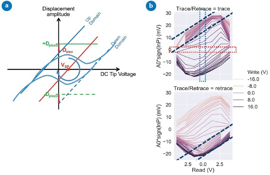
Figure 5. PFM response with applied bias on ferroelectric samples: (a) schematic of ferroelectric hysteresis without electrostatics (green), with electrostatics on a non-ferroelectric sample (red), and with both electrostatics and ferroelectric behavior (blue). (b) cKPFM plots from a ferroelectric material at different write voltages. The dashed black lines indicate the electrostatic response in the part of the hysteresis curve where the ferroelectric response of the sample is saturated. If the sample were an ideal dielectric, the red dashed box would indicate the surface potential for the sample which changes from one write voltage to the next due to charge injection from the tip. The blue dashed box indicates the PFM response for the off-field hysteresis loop. Data is from a PZT sample with DC voltage applied to tip, AC to sample. Image Credit: Bruker Nano Surfaces
The response data plots for each write bias are functions of the read bias results in a cKPFM plot.5
Figure 5b displays a cKPFM plot of data obtained on a ferroelectric (PZT). The electrostatic response is revealed by the tilt in the linear sections of the curve at the extremes of write bias, i.e., where the ferroelectric response is saturated, represented by black dashed lines. Contrastingly, the non-linearity evident in the cKPFM plots suggest a ferroelectric response.
For a dielectric material to be ideal, every plot would be linear, with the x-intercepts (denoted by the red box in Figure 5b) indicative of the sample’s surface potential following charge injection by the associated write segment. The y-intercepts (blue box) signal the PFM response for the off-field hysteresis loop.
For materials that are ferroelectric, it is challenging to distinguish the ferroelectric and electrostatic response due to the surface potential (and the electrostatic contribution to displacement) differences between write segments.
Even if one read voltage specifically cancels out the surface potential at the start of the measurement, it cannot continue for the whole hysteresis loop. To tackle this, Balke et al. utilized a mixture of on-field SS-PFM (for electrostatic slope and PFM response) and non-contact KPFM (for surface potential) with an identical write waveform.6
This was effective for PPLN with DC voltages lower than the coercive voltage (evading domain switching) but does not enable the whole hysteresis loop to be corrected.
Positioning the beam-bounce laser at the electrostatic blind spot
This third approach comprises utilizing sub-resonance PFM and cautiously positioning the beam-bounce laser to identify the deflection angle of the cantilever at the electrostatic blind spot (ESBS) for the lever.9
The ESBS is the position where the distributed electrostatic force applied to the cantilever does not affect its slope and, consequently, does not impact the deflection determined by the AFM.
This ESBS method is effective with both soft and stiff cantilevers but not for CR-PFM, where the shape of the cantilever is controlled by contact resonance behavior.
For frequencies that are significantly below contact resonance, the relative contribution of the electrostatic force to the slope of the cantilever is dependent on the location along the cantilever that it is measured.
For the majority of cantilevers, the ESBS is positioned approximately two-thirds of the way along the cantilever (from the base to the tip), although the exact position relies on the contact stiffness.
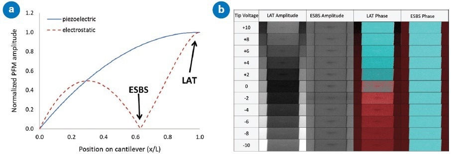
Figure 6. The effect of electrostatic force on the cantilever depends on beam-bounce laser position: (a) the electrostatic force on the cantilever has minimal influence on the cantilever deflection when the laser is positioned at the electrostatic blind spot (ESBS, see red-dashed line), (b) PFM maps of amplitude (left) and phase (right) collected at different tip voltages on PPLN demonstrate the significant variation in response with surface potential when the laser is positioned at the tip (LAT) and the improvement possible with the ESBS. Image Credit: Bruker Nano Surfaces
Figure 6a conveys the impact of distributed force on the cantilever (electrostatic) and pure tip displacement (piezoelectric). PFM is vulnerable to the sum of the slope from the two sources, and therefore, placing the laser at the ESBS will cause substantially less electrostatic artifact than the typical laser at tip (LAT) position.
For optimal performance, the laser position is adjusted iteratively until one of the following occurrences take place:
- Amp|↑domain = Amp|↓domain for a sample where this is anticipated (such as PPLN);
- Amp is minimized on a non-piezoelectric sample;
- ∂Amp/∂VDC is minimized.
Figure 6b presents PFM images obtained on PPLN at varying tip voltages, utilizing a Bruker SCM-PIT-V2 probe with spring constant kc = 2.7 N/m. The two leftmost columns detail PFM amplitudes at the ESBS and LAT, while the rightmost columns detail the PFM phase.
The ESBS amplitude of the center domain is equivalent to the outer domains over tip voltages from -10 V to +10 V, as expected, but there is a broad range of amplitude for LAT. Similarly, the ESBS phase is notably consistent across the voltage range, but this is not the case for LAT.
Calculating this for the ESBS case, it is determined that d33=10.7±0.9 pm/V for the left domain and 9.3±0.3 pm/V for the central domain. The result of positioning the laser at the end (LAT) is d33=12.4±6.6 pm/V for the left domain and 5.9±2.8 pm/V for the central domain, which is a difference of more than a factor of two.
The variation is more severe in the phase channel. For ESBS, the phase difference amongst domains ranges from +178.1° to +179.9° (with the expected value of +180°). In comparison, the LAT phase difference varies from -15.3° to +201.4°.
These results show that simply positioning the laser at the ESBS almost fully removes the electrostatic component of the PFM signal.
The combination of sub-resonance PFM with SS-PFM, either LAT or laser at ESBS, enables the effect of imposed electrostatics to be observed (via the read bias) on PFM spectra.
Figure 7 presents PFM amplitude ‘butterfly loops’ on a PZT thin film with write voltages from -11 V to +11 V. To observe the effect of the electrostatic force on the measurements, the read voltages also differed from -2.7 to +2.7 V.
In Figure 7a (LAT), the loop for read (0 V) is the only result that has the typical symmetric loop. All the other results are skewed in one direction or another. In comparison, Figure 7b (laser at ESBS) created loops that are relatively consistent up to ±1.8 V.
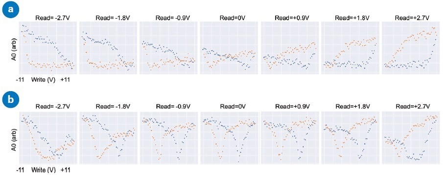
Figure 7. Investigating the influence of beam-bounce laser position on PFM response using sub-resonance SS-PFM; (a) PFM amplitude vs. write voltage spectra (‘butterfly loops’) at different read voltages with laser positioned near the end of the cantilever (LAT). (b) PFM spectra at different read voltages with laser positioned at the electrostatic blind spot (ESBS). Sample: PZT; Probe: SCM-PIT-V2. Image Credit: Bruker Nano Surfaces
Mapping Ferroelectric Parameters
If spectroscopy is performed at various locations across a surface, a map of any given parameter from the hysteresis loop can be produced.10 Figure 8a shows an analysis of a single piezoelectric loop (top) to acquire a ferroelectric parameter at a given point.
This analysis is replicated for each point in a 20x20 array, and maps of coercive voltages V0+ and V0- are produced (bottom). This mapping is carried out utilizing MIROView™, permitting the array to be located alongside other AFM measurements (adhesion, topography, elastic modulus, dissipation, etc.), formerly poled regions, or optical images.
Figure 8b compares a CR-PFM phase image obtained after the spectroscopic map displaying poled regions with the positive coercive bias by overlapping a contour line map with constant V0+. This form of correlation may be utilized to study the effect of nanostructures, such as grain boundaries and defects, on the material’s ferroelectric behavior.
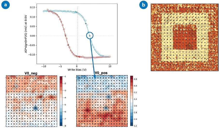
Figure 8. Maps of ferroelectric properties can be extracted from arrays of spectra: (a) top is a ferroelectric hysteresis loop from resonant SS-PFM on PZT, in (a)bottom key parameters such as coercive voltages V0+ and V0- are extracted from the loops and mapped; (b) V0+ map is overlaid upon a subsequent PFM phase map to look for influence of domain structure on coercive voltages. Image Credit: Bruker Nano Surfaces
PeakForce Tapping® may be utilized to locate the region of interest instead of contact mode, further preserving the tip and preventing damage to the most sensitive samples.
If superior levels of detail are needed, MIROView allows arrays in sizes up to 50x50 = 2500 spectra of 10 to 20 MB each, developing a full data set of 25 to 50 GB.
Collating such vast amounts of data is a lengthy process, but Bruker’s DSP-based RampScripting reduces the total acquisition time by removing system latencies between distinct segments in the script (where switching times are on the order of 10 µs).
Conclusions
Several challenges exist concerning the collection and analysis of quality PFM data, but the sensitivity and resolution of the AFM make it a powerful option for examining ferroelectric materials.
If compensation is considered for electrostatics and instrumental artifacts, results are able to be evaluated across different types of instruments and labs, and the progress of structure-property relationships are assisted.
Bruker’s SS-PFM and DCUBE PFM both work with either sub-resonance or contact resonance PFM and can be used with PeakForce Tapping to allow survey scanning, eliminating contact mode and its associated lateral forces.
They allow for the interrogation of fragile samples, deliver more repeatable results, and enable the use of stiffer levers, reducing electrostatic artifacts.
Key practical solutions
- If coercive voltages are low or the sample response is weak, contact resonance is advised to maximize signal-to-noise, but cautious analysis is required for response amplitude quantification. When sample response is greater, sub-resonance PFM is the most direct approach to attain quantitative amplitude data (and d33).
- By poling a sample with an established electrostrictive coefficient sign, calibration of the system phase offset is possible at a particular frequency, enabling accurate interpretation of spectroscopic data.
- The electrostatic force on the cantilever may produce a PFM artifact that is extremely like the ferroelectric response. For sub-resonance PFM, this is alleviated by locating the beam-bounce laser at the electrostatic blind spot (ESBS) on the cantilever.
- SS-PFM may be utilized to examine the impact of electrostatics on the PFM spectra for both resonance and sub-resonance PFM, with the use of various read voltages.
- Arrays of SS-PFM spectra are able to be analyzed and utilized to create maps of key ferroelectric parameters, allowing correlation with nanostructures at the sample surface.
Acknowledgments
The authors of the original article DOI: 10.13140/RG.2.2.19958.88648 give thanks to Jason Killgore (NIST) and Liam Collins (ORNL) for discussions and clarifications, which allowed this article to be significantly improved.
References and Further Reading
- Kalinin, S. v., Rodriguez, B. J., Jesse, S., Shin, J., Baddorf, A. P., Gupta, P., Jain, H., Williams, D. B., & Gruverman, A. (2006). Vector Piezoresponse Force Microscopy. Microscopy and Microanalysis, 12(03), pp. 206–220. https://doi.org/10.1017/S1431927606060156
- Hidaka, T., Maruyama, T., Saitoh, M., Mikoshiba, N., Shimizu, M., Shiosaki, T., Wills, L. A., Hiskes, R., Dicarolis, S. A., & Amano, J. (1996). Formation and observation of 50 nm polarized domains in PbZr 1− x Ti x O 3 thin film using scanning probe microscope. Applied Physics Letters, 68(17), pp. 2358–2359. https://doi.org/10.1063/1.115857
- Jesse, S., Baddorf, A. P., & Kalinin, S. v. (2006). Switching spectroscopy piezoresponse force microscopy of ferroelectric materials. Applied Physics Letters, 88(6), p. 062908. https://doi.org/10.1063/1.2172216
- Vasudevan, R. K., Balke, N., Maksymovych, P., Jesse, S., & Kalinin, S. v. (2017). Ferroelectric or non-ferroelectric: Why so many materials exhibit “ferroelectricity” on the nanoscale. Applied Physics Reviews, 4(2), p. 021302. https://doi.org/10.1063/1.4979015
- Balke, N., Maksymovych, P., Jesse, S., Herklotz, A., Tselev, A., Eom, C.-B., Kravchenko, I. I., Yu, P., & Kalinin, S. v. (2015). Differentiating Ferroelectric and Nonferroelectric Electromechanical Effects with Scanning Probe Microscopy. ACS Nano, 9(6), pp. 6484–6492. https://doi.org/10.1021/acsnano.5b02227
- Balke, N., Jesse, S., Yu, P., ben Carmichael, Kalinin, S. v, & Tselev, A. (2016). Quantification of surface displacements and electromechanical phenomena via dynamic atomic force microscopy. Nanotechnology, 27(42), p. 425707. https://doi.org/10.1088/0957-4484/27/42/425707
- Neumayer, S. M., Saremi, S., Martin, L. W., Collins, L., Tselev, A., Jesse, S., Kalinin, S. v., & Balke, N. (2020). Piezoresponse amplitude and phase quantified for electromechanical characterization. Journal of Applied Physics, 128(17), p. 171105. https://doi.org/10.1063/5.0011631
- Kim, S., Seol, D., Lu, X., Alexe, M., & Kim, Y. (2017). Electrostatic-free piezoresponse force microscopy. Scientific Reports, 7(1), p. 41657. https://doi.org/10.1038/srep41657
- Killgore, J. P., Robins, L., & Collins, L. (2022). Electrostatically-blind quantitative piezoresponse force microscopy free of distributed-force artifacts. Nanoscale Advances, 4(8), pp. 2036–2045. https://doi.org/10.1039/D2NA00046F
- Jesse, S., Lee, H. N., & Kalinin, S. V. (2006). Quantitative mapping of switching behavior in piezoresponse force microscopy. Review of Scientific Instruments, 77(7), p. 073702. https://doi.org/10.1063/1.2214699

This information has been sourced, reviewed and adapted from materials provided by Bruker Nano Surfaces .
For more information on this source, please visit Bruker Nano Surfaces .