Scanning probe microscopy (SPM) is a set of advanced methods for surface analysis. The recent advances in SPM of metals, polymers, insulating, and semiconductive materials are primarily due to the development of atomic force microscopy (AFM).
AFM is a powerful device for acquiring information about material surface structures at the nanoscale. It can be used to measure inorganic materials, including semiconductors and metals, as well as organic materials and biomaterials.
AFM patterning and imaging methods are widely utilized to carry out research into the fabrication of nanoscale devices. AFM involves the sample surface being scanned with a probe comprised of a sharp tip and a miniature cantilever.
When using AFM contact mode for imaging, the tip apex is in constant contact with the surface, while for tapping mode, it is in intermittent contact with the surface.
Conducting imaging using AFM for high-aspect-ratio nanostructures with straight walls and sharp edges in nanoscale metrology is complex due to the conical geometry and mechanical properties of most commercially available tips.
Nanowires Improve AFM Probe Functionality
One-dimensional (1D) semiconductor nanostructures are generally defined as linear structures with a diameter of less than 100 nm, such as nanotubes and nanowires. Due to their unique chemical and physical properties, they hold great potential as building blocks for the next generation of electronic and optoelectronic nanodevices.
For nanoscale metrology of high-aspect-ratio structures, gallium nitride (GaN) nanowires are embedded into probes to improve AFM imaging resolution.
These nanowires also allow the combination of AFM with other tools, including near-field scanning optical microscopy (NSOM) and scanning tunneling microscopy (STM), to provide a universal multipurpose probe. This combination may be employed to improve microscopy and lithography methods.
AFM Tips for Lithography: Laser Scanning Plus Spectroscopy
Groundbreaking research involving GaN nanowires and lasers on AFM probes for utilization in semiconductor patterning provides more significant opportunities to record a material's topography and fluorescence signal.
The Busani Research Group at the University of New Mexico (Albuquerque, NM) is carrying out research with 1D nanostructured materials, near-field spectroscopy, nanomembranes and nanolasers, and their integration into multifunctional devices.
The research group’s multidisciplinary research includes silicon photonics and photovoltaics and the application of data science methods in semiconductor research.
The group investigates and fabricates probes and lasers utilized in spectroscopic surface metrology for subnanometer inline lithography.
They have developed an AFM tip comprising a GaN nanowire and laser mounted on the probe to facilitate traditional laser scanning along with spectroscopy to record the material's fluorescence signal, as shown in Figure 1.
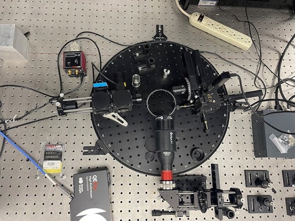
Figure 1. The Busani Research Group’s AFM probe for semiconductor patterning, equipped with an aluminum nitrate laser nanowire used as a lithographic tip, allows traditional laser scanning to be performed along with spectroscopy to record the fluorescence signal of the material. Image Credit: Busani Research Group
Busani’s research group combines AFM with a laser tip to probe physical processes and molecular forces.
When using the AFM probe for measuring the topography of a surface, the external laser can activate the nanowire through an integrated waveguide to enable the tip to become a laser source. This allows it to be used to radiate the material surface.
The AFM probe subsequently collects the light through the waveguide integrated on the silicon probe, to which the nanowire is attached.
The patterning process used is field-emission scanning probe lithography (FE-SPL), which is a high-resolution technique for nanofabrication. This process is based on the emission of electrons from ultrasharp tips positioned near a sample (distances less than 100 nm), with the emitted electrons exposing an ultrathin film.
The research group conducts nanofabrication, writing patterns in real-time, as well as masked lithography alignment. The nanowire employed as a lithographic tip facilitates self-alignment and dual lithography using either the emission of light or electrons.
Vibration Isolation
Ground vibration is crucial when dealing with nanostructures. Busani explains, “We needed an antivibration system for two reasons: for our laser optics, and for our AFM system that we integrate with an external laser source. The sample that gets exposed to the laser beam on the AFM needs to be optically stable.”
Busani’s research group introduced negative-stiffness vibration isolators in January 2022. These were created by Minus K Technology, an OEM supplier to manufacturers of scanning probe microscopes, micro-hardness testers, and other vibration-sensitive instruments and equipment, as displayed in Figure 2.
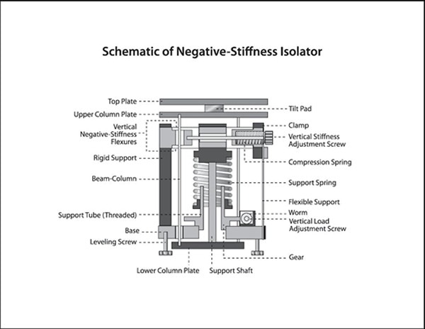
Figure 2. Schematic of the Minus K Technology negative-stiffness isolator. Image Credit: Minus K Technology
These vibration isolators have a small footprint and do not need compressed air or electricity, allowing sensitive instruments to be located wherever they may be required. There are no motors, chambers, or pumps involved, resulting in no required maintenance as there is nothing to wear out. They operate in a completely passive mechanical mode.
Negative-stiffness isolators attain a high level of isolation in numerous directions and provide the flexibility of custom tailoring resonant frequencies to 0.5 Hz vertically and horizontally (with some versions at frequencies of 1.5 Hz horizontally).
Considering an isolation system with a 0.5 Hz natural frequency, isolation starts at 0.7 Hz and improves as the vibration frequency increases. The natural frequency is typically utilized to describe the performance of the system.
Erik Runge, Vice President of Engineering at Minus K Technology, explains, “Vertical-motion isolation is provided by a stiff spring that supports a weight load, combined with a negative-stiffness mechanism.”
The net vertical stiffness is made very low without affecting the static load-supporting capability of the spring. Beam-columns connected in series with the vertical-motion isolator provide horizontal-motion isolation, and a beam-column behaves as a spring combined with a negative-stiffness mechanism. The result is a compact passive isolator capable of very low vertical and horizontal natural frequencies and high internal structural frequencies.”
Erik Runge, Vice President of Engineering, Minus K Technology
Negative-stiffness isolators have a high performance, which is measured using a transmissibility curve. Vibration transmissibility measures the vibrations that are transmitted through the isolator relative to the input vibrations.
When negative-stiffness isolators are adjusted to 0.5 Hz, they achieve approximately 93% isolation efficiency at 2 Hz, 99% at 5 Hz, and 99.7% at 10 Hz.
“The negative-stiffness vibration isolation is used for the laser setup to reduce vibration and micromovement,” Busani explains.
“Stabilizing the sample is critical to reducing noise. The isolator gives better procedural alignment on the tip and allows us to reduce the testing time. Negative-stiffness vibration isolation provides the support needed for the probe’s precision operation,” he concludes.
Acknowledgments
Produced form materials originally authored by Jim McMahon at Zebra Communications.

This information has been sourced, reviewed, and adapted from materials provided by Minus K Technology.
For more information on this source, please visit Minus K Technology.