Sponsored by PerkinElmerReviewed by Olivia FrostAug 23 2023
Silicon wafers are processed by adding dielectric films, which are primarily utilized to isolate circuits and offer mechanical and chemical protection to the device. These films also serve as masking materials during wafer fabrication.
Various film substrates are available, but borophosphosilicate glass and silicon nitride (Si3N4) are two of the most common examples. Silicon nitride thin films hold considerable scientific interest across multiple application fields.1
In addition to the properties required for electronics manufacturing, they also provide excellent optical, mechanical, and thermal properties, meaning that they can be used in solar cell applications where they serve as antireflection and passivating coatings.1

Image Credit: ShutterStock/Dave Weaver
The films are created using various deposition techniques, each of which influences the quality of the silicon nitride. The process can introduce hydrogen into the film through the silane and ammonia reactants. A high hydrogen content can impact film properties and performance. Furthermore, the optical properties of the nitride film rely on the ammonia-to-silane ratio.
FTIR (Fourier transform infrared) spectroscopy is widely employed in the electronics and solar industries to determine material chemical properties. This article outlines the FTIR method used to measure and compute the -NH and -SiH content in Si3N4 films.
Experimental
FTIR measurements can be conducted on silicon wafers to serve various applications, allowing for measurements in either transmission or reflectance modes.
The analysis is performed through transmission when examining silicon nitride films on silicon wafers. The wafers are positioned within the MappIR system within the PerkinElmer Spectrum 3™ FTIR spectrometer, as depicted in Figure 1.
The measurement setup consists of a PerkinElmer Spectrum 3 FTIR spectrometer coupled with a Pike MappIR (or Mapp300) wafer holder and optical system, complete with automation software. This system can examine wafer sizes ranging from 2 to 8 inches (MappIR) or 12 inches (Mapp300) in transmission and reflection modes.
Through automation software, seamless and unattended wafer mapping is achievable, allowing for data collection from across the entire wafer based on predetermined or user-defined mapping arrangements. Data collection is followed by calculations based on the analysis method specified.
Spectra were collected in transmission mode for 8-inch diameter silicon wafers coated with a silicon nitride film at a spectral resolution of 4 cm-1. The data collection process took place over a period of four scans.
Figure 2 shows the spectra of an uncoated wafer and a wafer coated with a thin Si3N4 dielectric film layer. Evident disparities exist between these two spectra, highlighting distinct spectral bands attributed to the presence of Si-H and N-H at 2170 cm-1 and 3350 cm-1, respectively, as shown in Figure 3.
The calculation methodology employed in this article is based on the Lanford and Rand method.2 Peak areas are computed by incorporating suitable baseline regions to compensate for spectroscopic baseline effects effectively.
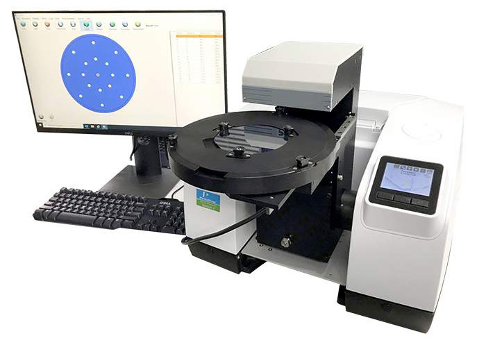
Figure 1. The Spectrum 3 FTIR MappIR System. Image Credit: PerkinElmer
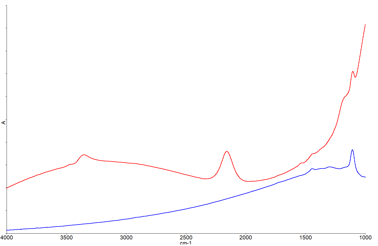
Figure 2. Spectra of Uncoated Silicon Wafer (blue) and Wafer with Si3N4 film (red). Image Credit: PerkinElmer
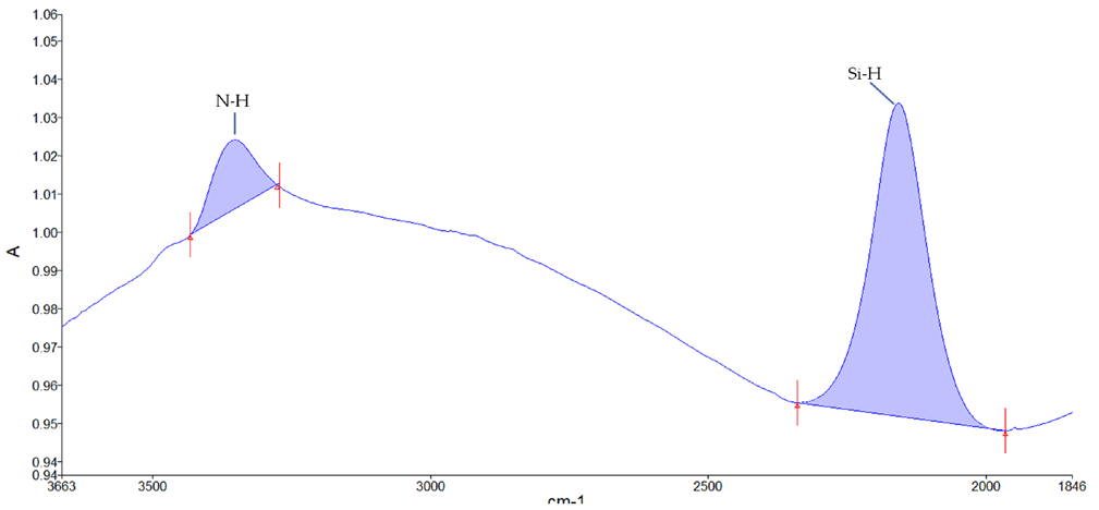
Figure 3. Spectral ranges used for the Si-H and N-H concentration calculations. Image Credit: PerkinElmer
Calculations
Calculation methods from the paper “The hydrogen content of plasma-deposited silicon nitride,” by Lanford and Rand are outlined below.2
Number of Si-H bonds/cm3 = K1 x (peak area of Si-H)/thickness
Number of N-H bonds/cm3 = K2 x (peak area of N-H)/thickness
Where K1=1.36 x 10¹⁷ and K2=1.904 x 10¹⁷
K1 and K2 Values from literature.2 K2/K1=1.4 and accounts for relative absorption coefficients of Si-H and N-H
Si-H % = (Si-H atom)/ [(film density x 3.035 x 10²²) + (Si-H atom) + (N-H atom)]
N-H % = (N-H atom)/ [(film density x 3.035 x 10²²) + (Si-H atom) + (N-H atom)]
Film Thickness 8500A
- Si-H bonds/cm3 = K1 x (peak area of Si-H)/thickness = 1.5744 x 10²² bonds/cm3
- N-H bonds/cm3 = K2 x (peak area of N-H)/thickness = 0.4883 x 10²² bonds/cm3
- Si-H% = (Si-H atom)/ [(film density x 3.035 x 10²²) +(Si-H atom) + (N-H atom)] =1.5744 x 10²²/ [(2 x 3.035 x 1022) + 1.5744 x 10²² + 0.4883 x 10²²] = 19.36%
- N-H% = (N-H atom)/ [(film density x 3.035 x 10²²) +(Si-H atom) + (N-H atom)] =0.4883 x 10²²/ [(2 x 3.035 x 1022) + 1.5744 x 10²² + 0.4883 x 10²²] = 6.00%
Conclusion
Using the MappIR system, FTIR spectroscopy has proven to be a rapid and straightforward approach for determining the hydrogen content within silicon nitride films.
This technique can be applied in studies related to film deposition procedures, facilitating the enhancement of film characteristics for optimal utilization in semiconductor or solar cell applications.
References
- Alain E. Kaloyeros et al 2020 ECS J. Solid State Sci. Technol. 9 063006.
- William A Lanford, M J Rand, Journal of Applied Physics, volume 49, 1978, pages 2473–2477.

This information has been sourced, reviewed and adapted from materials provided by PerkinElmer.
For more information on this source, please visit PerkinElmer.