Sponsored by PerkinElmerReviewed by Olivia FrostAug 20 2025
Semiconductors are routinely used in a growing list of everyday devices and machines, including computers, phones, TVs, public transport, and cars. They are integral to many current applications, and their importance and applicability are increasing. For instance, a single electric car requires as many as 3,000 semiconductors.
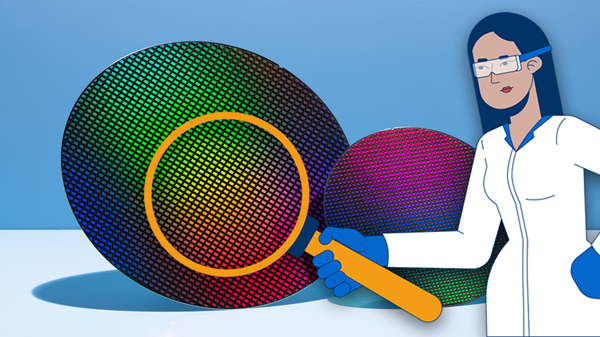
Image Credit: PerkinElmer
Stringent conditions are required during semiconductor manufacture to prevent materials from becoming contaminated, which can result in diminished performance. Even small traces of contamination can have a serious impact on semiconductor performance.
This article examines sources of contaminants in typical semiconductor manufacturing settings and the necessary testing requirements and systems to minimize them.
During semiconductor manufacturing processes, there are several opportunities for contamination, and it is important that all areas are carefully managed to ensure that semiconductor materials are not compromised.
Semiconductors are manufactured from silicon, one of Earth's most abundant metalloid elements. Silicon must be refined to 99.99999…% purity before use in various applications, and materials must be thoroughly tested for impurities to parts per quadrillion before use.
The presence of contaminants or defects during the fabrication phase can also cause issues. Every component material in a semiconductor, from silicon to water, chemicals, and gases, must be thoroughly inspected and monitored.
The product supply chain has been functioning less effectively since the COVID-19 pandemic due to production facilities and workplaces shutting down worldwide at various points over the last three years.
Shortages and delays of components and raw materials, key to semiconductor production, have also intensified demand. Even missing a single component or part means a product cannot be finished. While the situation is beginning to improve and stocks are again building up, extended timelines are still in place for delivering some devices requiring semiconductors.
Manufacturers face additional pressure to meet surging demand while dealing with delays in the wider supply chain and shortages of raw materials.
Manufacturers may attempt to expedite the semiconductor manufacturing and fabrication processes by implementing less stringent controls, but any attempt to cut corners can significantly reduce the quality of materials by increasing the risk of components coming into contact with contaminants.
To ensure the quality of semiconductor materials, strict environmental controls must be in place throughout manufacturing and fabrication. These controls must be implemented in conjunction with rigorous testing protocols that can detect and address any impurities or contaminants.
Sources of Contamination in Semiconductor Materials
There is a wide range of potential contaminants at every stage of the manufacturing and fabrication processes, with common contaminants originating from organic compounds, metals, and ions. There are also potential gaseous and particle impurities in gases, as well as potential dissolved or particle impurities in chemical solutions.
Contaminants can come from the environment, raw materials, gases, chemicals, equipment, filters, and tubing. Contact with humans can also lead to contamination, even when working in cleanroom environments.
Katsu Kawabata, president of Japan-based IAS Inc., explains, “Contamination sources are everywhere. At all steps, there is a possibility of contamination. Even the cleaning process can also be a source of contamination.”
Sourcing materials or components from different manufacturers for different parts of the production process creates opportunities for contamination, because this limits the manufacturer’s capacity to implement consistently strict controls.
Environmental controls play a central role in reducing contamination opportunities. For example, previous decades saw semiconductor fabrication using open cassettes for wafers between 6 and 18 inches. High-end semiconductor devices now use a completely sealed cassette known as FOUP, significantly limiting contaminants’ ability to come into contact with materials.
“It’s very effective, because in the normal environment, even if you have a clean room, human beings are big particle generation sources. If someone walks around and some particles are generated, then this particle may deposit on the wafer,” adds Kawabata. “That’s why such growth of this new kind of environment is very important.”
Semiconductor Testing Solutions
Rigorous environmental controls are an essential element of modern semiconductor manufacturing processes, and several testing solutions are key to the detection of impurities and contaminants.
XRF techniques are routinely used in the measurement of metallic impurities, but these methods have some limitations in terms of their effectiveness. “Metallic impurities can be analyzed by TRX-RF and VPD-ICP-MS. Organic compounds are analyzed by GC-MS. Ionic impurities are analysed by IC,” Kawabata adds.
Contamination levels can vary depending on the device. Image sensor CMOS testing necessitates the lowest level of contamination controls and does not require the use of destructive testing processes.
PerkinElmer is a widely recognized provider of semiconductor testing systems for contaminants and impurities. Its NexION® 5000 is a multi-quadrupole ICP mass spec system that employs four quadrupoles, despite some detection systems relying on an octopole and hexapole for a reaction cell to remove interferences.
Kawabata explains, “The performance is quite similar in terms of interference removal, but PerkinElmer has one strong feature of this quadrupole. When many high-purity materials are analysed, a lot of main materials are introduced into the ICP-MS.”
“For example, laser ablation ICP-MS introduces solid materials into the ICP-MS, and it requires the measurement of major elements. So, huge amounts of major elements are introduced into the ICP-MS, giving very high signals. If it is analysed normally, the detector of the ICP-MS is saturated.”
“However, the PerkinElmer ICP-MS can easily reduce the sensitivity of only one element by using the reaction quadrupole.”
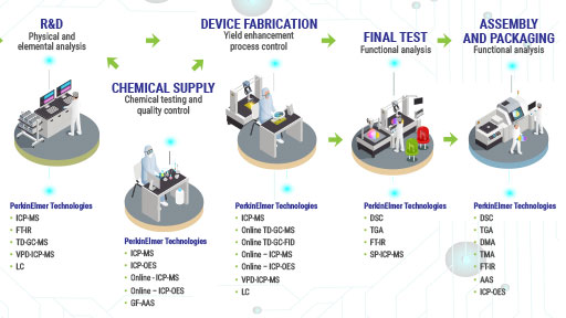
Image Credit: PerkinElmer
Acknowledgments
Produced from materials originally authored by PerkinElmer.

This information has been sourced, reviewed and adapted from materials provided by PerkinElmer.
For more information on this source, please visit PerkinElmer.