Silicon carbide (SiC) is a wide-bandgap semiconductor material utilized in high-power, high-temperature, and high-frequency electronic devices. 4H-SiC substrates have distinct characteristics, including elevated thermal conductivity, high breakdown voltage, and superior chemical inertness, making them perfect for power electronics, radio frequency devices, and sensors.
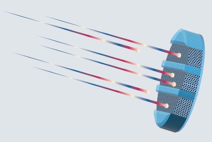
Ion implantation is crucial for fabricating SiC devices (Figure 1) and requires meticulous control over dopant distribution. Precise characterization of the wafer offcut or miscut angle is pivotal for achieving high device performance and reliability.
Bruker’s QCVelox high-resolution X-ray diffraction (HRXRD) system is a robust instrument for determining the offcut angle with precision, maximizing the ion implantation process for 4H-SiC substrates.

Figure 1. Representation of the ion implantation process on SiC power device. Image Credit: Bruker Nano Surfaces and Metrology
Importance of Accurate Offcut Angle in 4H-SiC in Ion Implantation
The offcut angle of a 4H-SiC substrate plays a central role in calculating the quality and performance of SiC devices. Defects in SiC occur alongside the growth direction. Due to this, an intentional offcut is imparted on SiC substrates to protect the underlying 4H-SiC crystal and allow the defects to have a predictable orientation throughout epitaxial growth.
Precise offcut angle control is critical for crystal quality, channel suppression, and defect engineering precision.
Crystal Quality
- Reducing Defect Density: Precise offcut guarantees high crystal quality, diminishing defect density and improving device reliability.
- Enhancing Material Uniformity: Precise offcut results in uniform epitaxial growth and crystal morphology, enhancing material quality and device performance.
Channeling Suppression
- Improving Ion Implantation Precision: Precise offcut maximizes ion implantation, diminishing ion channeling risk and improving device performance.
- Guaranteeing Uniform Dopant Distribution: Accurate offcut guarantees uniformity in ion implantation, reducing channeling effects and enhancing device uniformity.
Defect Engineering Precision
- Improving Dopant Activation: Precise offcut facilitates controlled defect engineering, maximizing dopant activation and enhancing device performance.
- Improving Device Reliability: Accurate offcut facilitates the generation of customized defect profiles, improving device reliability and durability in 4H-SiC-based electronics.
Although offcut is critical for both Si and SiC wafers, its precision is also crucial due to its heightened sensitivity to crystal defects. The offcut angle in Si wafers impacts crystal defects and dislocations.
The effect is typically less drastic than that of SiC due to the broader bandgap in SiC and elevated operating temperatures, where defects spread and result in a higher density of crystallographic and surface defects.
Accurate offcut in SiC is critical for device performance and reliability, as it reduces defects and guarantees high crystal quality.
Role of HRXRD in 4H-SiC Ion Implantation
HRXRD provides multiple benefits for precisely and accurately assessing wafer offcut angles in 4H-SiC substrates, such as:
- High Precision: HRXRD offers accurate assessments of lattice orientation and offcut angles (magnitude and direction) with sub-degree resolution, guaranteeing the precise detection of small deviations in the expected 4H-SiC wafer orientation.
- Non-Destructive Analysis: HRXRD enables the characterization of wafer offcut without damaging the sample, allowing for in-line metrology.
- Versatility: HRXRD can be applied to multiple SiC substrates with diverse orientations, sizes, doping levels, and polytypes, making it flexible for numerous SiC device fabrication processes.
Bruker HRXRD for Rapid Offcut Determination
HRXRD is a power reference metrology approach in silicon and compound semiconductor manufacturing.
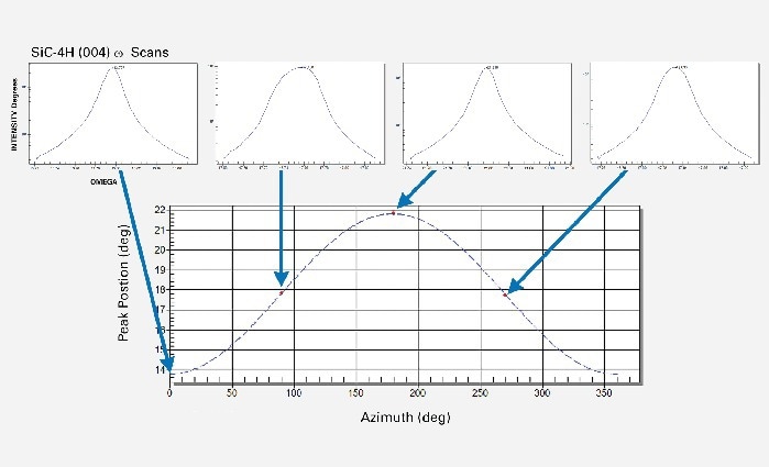
Bruker’s sophisticated HRXRD systems allow an extra level of sensitivity to discrete variations in wafer offcut, with unparalleled precision and accuracy reached by assessing various high-resolution rocking curves (ω scans) at various azimuth (φ) angles to quantify both the offcut magnitude and direction from the diffracted angles, as displayed in Figure 2.
This sequence of assessments is completely recipe-driven, and analysis can be automated using the Bruker analytical software.

Figure 2. Illustration of the offcut calculation by measuring ω rocking curves at different wafer azimuth within the recipe. Image Credit: Bruker Nano Surfaces and Metrology
If the nominal wafer thickness and expected offcut data are given as a reference for offcut refinement, precise offcut assessments could be enhanced and performed more quickly. This is particularly beneficial in high-volume manufacturing, where the nominal wafer thicknesses and offcuts are well-controlled.
Recent tests undertaken on a dedicated high-intensity Bruker QCVelox HRXRD diffractometer displayed how a typical 200 mm 4H-SiC wafer with an expected 4 ° offcut can be assessed in less than 60 seconds with accuracy and precision of <0.005 ° for offcut magnitude and <0.01 ° for offcut direction compared to the conventional approach displayed in Figure 2.
This method is appropriate for characterizing all common semiconductor substrates, such as SiC, Si, GaAs, InP, and GaN.
Optimize Ion Implantation by Leveraging HRXRD
Ion implantation is crucial in 4H-SiC semiconductor manufacturing and necessary for precise control over dopant distribution and device properties.
By using HRXRD for accurate wafer offcut, semiconductor manufacturers can maximize ion implantation processes and improve device performance in 4H-SiC-based electronics, accelerating innovation and facilitating novel applications in the electronics industry.

This information has been sourced, reviewed, and adapted from materials provided by Bruker Nano Surfaces and Metrology.
For more information on this source, please visit Bruker Nano Surfaces and Metrology.