Optical lithography is employed in manufacturing integrated circuits. It starts with attaching a photosensitive material—or photoresist—to the substrate.
A photomask with the required pattern is placed on the photoresist, and light is emitted through the photomask, revealing certain regions of the photoresist.
These uncovered areas experience a chemical change, becoming soluble or insoluble in a developer solution. Following development, the pattern is transmitted onto the substrate via chemical vapor deposition, etching, or ion implantation.
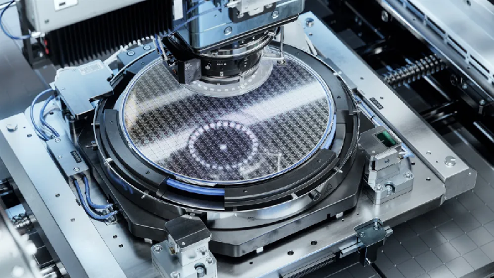
Image Credit: Optris GmbH & Co. KG
Lithography includes several important stages in which absolute temperature and temperature consistency are key. Firstly, the wafer is washed and coated with photoresist as a light-sensitive layer. This photoresist layer must be placed and then cured to eliminate solvents, a highly sensitive method to temperature fluctuations.
Keeping a homogeneous temperature distribution is pivotal to attaining a consistent layer thickness. Accurate understanding and surface temperature control are needed to guarantee stability and quality.
Once the photoresist is applied and cured, UV light is cast onto the wafer through a mask comprising the required pattern. The regions of the photoresist revealed to the UV light experience a chemical change. The wafer is then formed to uncover the pattern, with the exposed material eliminated via etching.
Maintaining precise temperature control during this procedure is essential. Any variation can cause faults in the pattern, impacting the final semiconductor devices’ performance and consistency. Temperature control is, therefore, fundamental to lithography and overall semiconductor manufacturing.
Temperature Control in Lithography with CSmicro Infrared Sensors
The wafer’s surface temperature must be assessed indirectly to prevent interference with the sensitive manufacturing process. Retaining a consistent temperature distribution is key to attaining a homogeneous layer thickness of the photoresist, and this must be assessed directly on the object.
A pyrometer with a long-wave spectral range (8–14 µm) is employed for this role. Space conditions are usually tight, so the sensor must be as small as possible to ensure correct positioning, preferably vertical to the wafer surface.
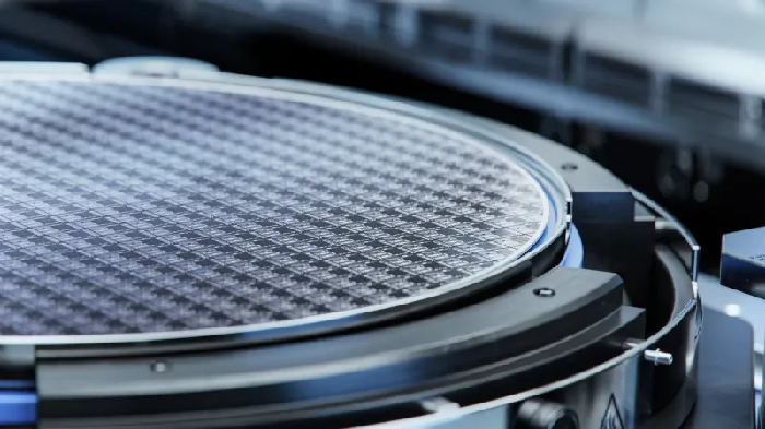
Image Credit: Optris GmbH & Co. KG
The CSmicro is the smallest infrared sensor series with the most compact sensor head and is perfect for this use. Produced by Optris, the CSmicro series is prominent because of its robust design and high accuracy.
It features a miniaturized sensor head for simple integration into enclosed spaces, making it ideal for semiconductor manufacturing settings.
The CSmicro sensors can measure temperatures ranging from –40 to 1030 °C, offering adaptability for numerous manufacturing steps. Their rapid response time guarantees real-time temperature observation and control.
This prompt feedback is crucial for retaining the tight temperature tolerances demanded in lithography. The temperature signal is transferred to the PLC by an analog signal, enabling seamless integration into existent process control systems.
The CSmicro’s advanced optics and high-quality calibration ensure precise and consistent measurements, improving process stability and quality in semiconductor manufacturing.

This information has been sourced, reviewed and adapted from materials provided by Optris GmbH & Co. KG.
For more information on this source, please visit Optris GmbH & Co. KG.