With easier access to chip aging data, researchers and startups could design electronics built to endure radiation for years.
 Laboratory test: Fraunhofer researchers measure test structures on a semiconductor wafer. Image Credit: ©Fraunhofer IIS, Foto: BLEND 3 Frank Grätz
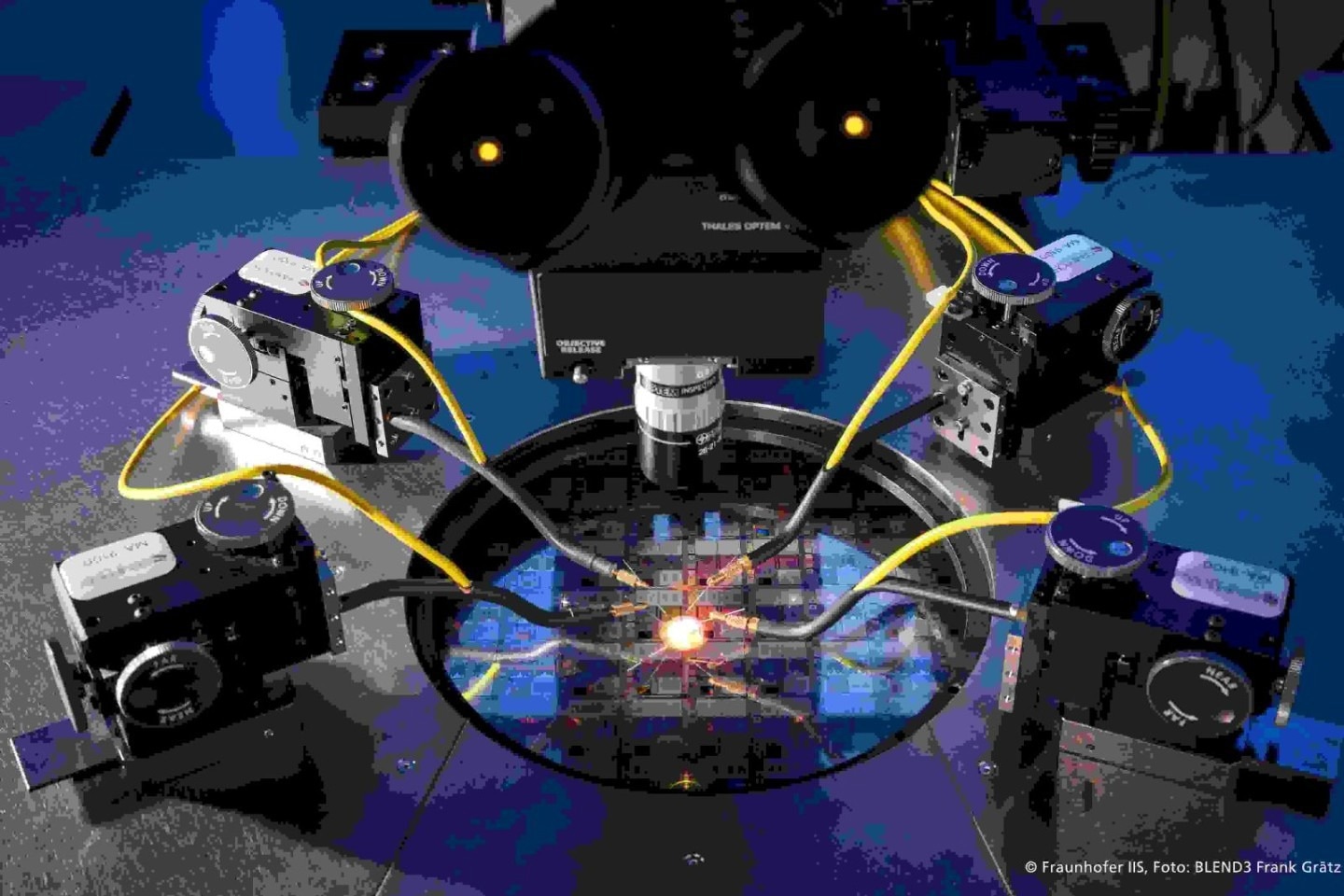
Researchers at the Fraunhofer Institute for Integrated Circuits IIS in Dresden are developing an open-source tool to enhance the prevention of radiation-induced functional degradation in electronic systems.
Electronic systems, when exposed to radiation, are susceptible to failure. This vulnerability is particularly critical for satellites and medical equipment, such as CT scanners.
The operation of modern services, such as telephone and television reception, GPS navigation systems, and broadband internet via satellite, is entirely dependent on electronics in space.
However, these components are particularly vulnerable to damage from cosmic radiation, which can lead to short-term failures, introduce malfunctions and memory errors, and accelerate the aging of the electronics.
Therefore, satellites, some of which are designed for several decades of operation in space, require exceptionally robust and radiation-resistant electronic designs. This same need for resilience applies to medical products, such as CT scanners, which use high-energy X-rays.
An Open-Source Tool Enables Access to Innovative Technologies
Achieving long-term circuit reliability requires the integration of semiconductor stress factors, such as radiation bombardment, into chip design during development.
However, doing so can be challenging for smaller companies and research institutions, due to the frequent absence of crucial data concerning the operational limits and characteristics of the components within these semiconductor chips.
This deficit often restricts their access to innovative technologies. Researchers at Fraunhofer IIS are collaborating with partners on a solution within the FlowSpace project.
We want to make electronics even more robust and reliable with an open-source tool.
Roland Jancke, Head, Design Methodology, Engineering of Adaptive Systems, Fraunhofer IIS
Jancke suggests that an open-source tool, combined with an open process design kit (PDK), could expand access to innovative technologies for communities such as universities and smaller companies.
An open PDK establishes a crucial interface between component technologists and chip designers. With freely available information regarding semiconductor components, designers gain insight into their behavior and potential applications.
This allows chip designers, for example, to factor in component aging during the initial design phase. In the FlowSpace project, Jancke's team conducts laboratory simulations to study the long-term response of components to radiation.
Scientists use mathematical models and measurements to realistically predict a component's likely aging process and its continued functionality after a decade of radiation exposure.
For applications exposed to radiation, chip developers commonly design critical circuit parts with redundancy to prevent malfunctions. Smaller solutions are gaining popularity due to their ability to conserve energy, space, and weight. This is especially significant for space modules.
The new solution allows for a reduction in the required chip area, as it is also compatible with increasingly smaller semiconductors that exhibit greater sensitivity to radiation.