Sponsored by Park SystemsReviewed by Olivia FrostJun 17 2025
This article introduces the FX200, the latest large-sample Atomic Force Microscope (AFM) from Park Systems, developed to meet both fundamental and advanced research requirements.
The FX200 is compatible with a broad range of sample types and sizes, providing an optimized solution for academic and industrial researchers engaged in pioneering discovery and innovation.
Introduction
Atomic Force Microscopy (AFM) has become an essential instrument in nanoscale surface characterization due to its outstanding spatial resolution, non-destructive measurement capabilities, and versatility across a variety of materials.
It is widely used in disciplines such as materials science, semiconductor research, and polymer analysis, offering crucial insights into surface morphology, mechanical properties, and functional characteristics at the nanometer scale.
Despite its advantages, traditional AFM operation involves significant challenges, mainly due to the manual intervention required for essential tasks such as probe exchange, cantilever detection, laser beam alignment, and parameter optimization.
These tasks demand a high level of expertise and require considerable time to execute proficiently, often leading to inconsistent measurement reliability and reducing throughput in research environments with high demand.
Overcoming these operational limitations is critical for the ongoing advancement of AFM technology. The future of AFM lies in the integration of sophisticated automation features that streamline workflows without compromising measurement precision.
Researchers should be able to collect high-quality, reproducible data with minimal manual involvement, enabling them to concentrate on data interpretation rather than complex system setup.
Park Systems’ FX product line represents this vision by incorporating advanced automation, including fully automated probe exchange, real-time cantilever detection, and intelligent laser beam alignment.
By significantly minimizing user intervention and reducing the potential for errors, the FX series improves both measurement efficiency and reliability, ushering in a new generation of high-performance, user-friendly AFM systems that allow researchers to focus exclusively on their scientific goals.
The FX200 inherits these strengths while providing an optimal platform for large-scale wafer-level measurements. Equipped with Macro Optics and an off-axis sample view camera, it enables researchers to view the entire sample at a glance, facilitating accurate and effortless measurement site selection.
In addition, advanced functionalities such as StepScan™ and programmable recipe-based measurement further extend the automation capabilities of the FX series.
These features enable researchers to specify measurement locations, configure custom parameters, and schedule repeated scans tailored to experimental requirements, significantly boosting workflow productivity and data reproducibility.
By integrating automation with user oversight, the FX200 establishes a new benchmark for high-throughput, precision AFM measurements, spanning from small sample sizes to full 200 mm wafer analyses.
One of Park Systems’ most notable user testimonials is, “If AFM had been known to be this easy, it would have been used much more often in most of my samples.”
While supporting users of the FX product line, Park Systems identified an additional need: providing researchers with comprehensive data logging and experimental archiving systems that not only expedite the collection of scientific data but also ensure a dependable, error-free digital laboratory recordkeeping process.
The following sections describe how these requirements are addressed.
Overview of FX200
The FX200 is Park Systems’ most recent large-sample AFM, developed to advance high-level research with enhanced automation capabilities, broad sample compatibility, and elevated performance (Figure 1).
What differentiates the FX200 from other large-sample AFMs is its accessibility to both seasoned AFM specialists and beginners, while consistently delivering high-quality results.
Striking a balance between maximum precision and fast operation, the FX200 demonstrates the effectiveness of performance optimization. Its user-friendly operation stems from decades of Park Systems’ expertise in designing automation and intuitive software for industrial in-line inspection AFMs.
The FX200 supports a wide spectrum of sample sizes, from a few centimeters up to complete 200 mm wafers. The sample surface can be easily examined and navigated using the integrated optical microscopy system. Target locations can be saved with a few clicks, enabling repeatable measurements at one or multiple sites.
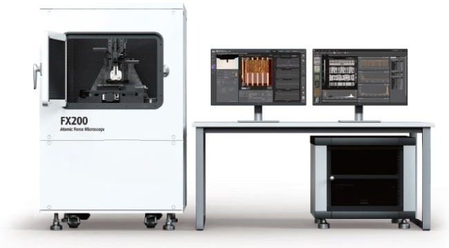
Figure 1. The full shot of FX200. The AFM system is located in an acoustic enclosure to minimize various noises. Image Credit: Park Systems
Key Features 1. Effortless Setup: AFM Probe Handling and Beam Alignment
A primary feature of the FX series is the automated probe identification and replacement system, along with automated beam alignment. These functions simplify the preparation process, which has traditionally made AFM operation difficult.
With minimal effort, researchers can bypass these complexities, making AFM techniques more accessible, even to new users.
The FX200 can store up to 16 AFM probes, providing excellent support for extended experiments involving large samples.
Each probe is identified using a QR code, allowing users to view all loaded probe types instantly. When a probe is selected, the FX200 automatically mounts it, detects the cantilever location, aligns the laser beam, and performs a frequency sweep with little user involvement.
In addition to convenience, the FX200 provides notable savings in both time and cost due to its automated tip exchange process. It eliminates the risk of damage to expensive probes by inexperienced users, thereby reducing unnecessary consumable expenses.
The time needed for training and practice is significantly minimized, as users are not required to manually mount a probe. Traditional setup procedures, including manual laser and cantilever alignment and PSPD adjustment, are particularly time-intensive for beginners.
By automating these processes, the FX200 enhances both efficiency and repeatability while lowering the threshold for nanoscale surface analysis.
Key Features 2. Improved Sample Navigation Optics with Large Field-of-View Camera
The FX200’s sample chuck can accommodate everything from small coupon-sized samples to 200 mm wafers. When paired with the large field-of-view camera, this allows users to quickly and easily identify regions of interest.
As shown in Figure 2, Park Systems’ SmartScan™ AFM control software displays a comprehensive image of the sample’s entire layout. The process is as follows:
- Use the Marker tool to locate the approximate region of interest.
- Use the mouse scroll to fine-tune and select the exact scan location. With enhanced optical capability, the FX series can resolve line widths down to 0.87 μm, improving the measurement experience.
- The positions added by the researcher for multiple measurements are also recorded as coordinates.
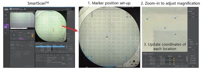
Figure 2. Macro optics for full 200 mm sample view. Image Credit: Park Systems
The multi-sample chuck supports loading of up to 16 coupon-sized samples, making it possible to perform comparative studies across varying conditions in a single session.
When used in combination with the FX200’s automatic probe exchange, this feature further streamlines the experimental process. Each sample is held in place with vacuum suction, minimizing the risk of movement or damage.
Key Features 3. StepScan: How is Automation Utilized in AFM?
The FX200’s automation features are central to simplifying AFM operation and improving user experience. StepScan enables straightforward automation of repeated measurements for research and industrial use cases.
With StepScan, researchers can conduct scans at multiple locations under identical or varied measurement parameters. Once positions and scan conditions are defined, as shown in Figure 3, the system can automatically switch probes and continue measurements across sites, as shown in Figure 4.
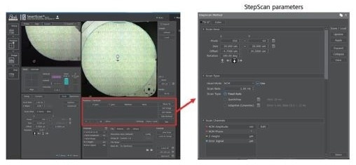
Figure 3. Captured SmartScan™ for StepScan and its parameters. Automatic sequential measurements at multiple predefined coordinates are possible by StepScan. Image Credit: Park Systems
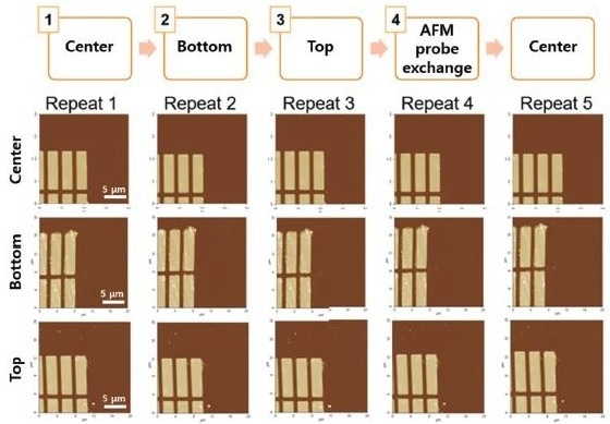
Figure 4. Repeated AFM results of each wafer position. Using StepScan, the center, bottom, and top positions of a 200 mm wafer are measured sequentially; following an AFM probe exchange, the process is repeated. Feature position across the wafer shows repeatability of ±2 μm. Image Credit: Park Systems
Key Features 4. From Large to Small
While user-friendliness is vital, AFM's primary value lies in its ability to produce accurate, high-performance results. The FX200 delivers exceptional resolution across various scales—from broad wafer overviews (100 μm × 100 μm) to intricate nanoscale features.
Figure 5 illustrates how the FX200 can zoom in from the general structure of a graphene flake to fine structural details. Moiré patterns in twisted bilayer graphene are clearly resolved at scan sizes of 100 nm × 100 nm or smaller.
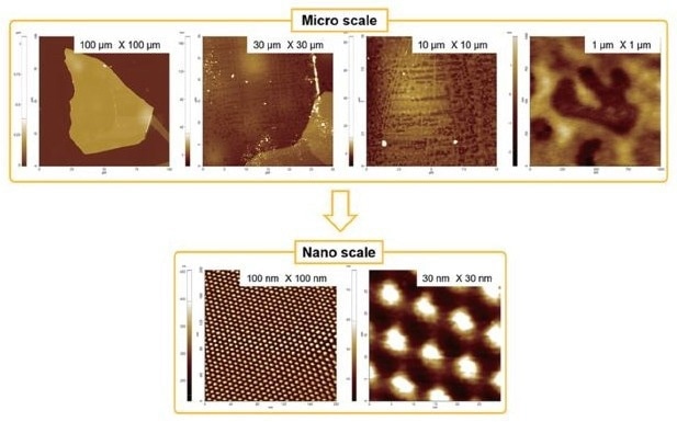
Figure 5. AFM results from 100 μm×100 μm to 30 nm×30 nm scan size. It covers a wide range of scan sizes from the entire structure of graphene flake to the moiré pattern of twisted bilayer graphene. Image Credit: Park Systems
Although designed for large samples, the FX200 excels at capturing small-scale features. As shown in Figure 6, it allows for nanoscale imaging in confined scan areas while preserving the larger structural context.
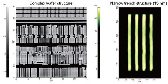
Figure 6. AFM results of Si wafer. It is possible to accurately measure the complex structure of Si wafer or the tiny and narrow trench structure. Image Credit: Park Systems
Key Features 5. Equipment Management
The FX200 is intended for deployment in academic research centers, industrial laboratories, and shared instrumentation facilities. As such, it ensures robust performance and safe operation across various use environments.
The FX200 monitors environmental conditions in real time through temperature and humidity sensors located near the AFM head. The data is displayed in graph form, as shown in Figure 7. If temperature or humidity values exceed acceptable thresholds (Temperature: 18 °C to 40 °C; Humidity: 30 % to 60 %), the system issues an alert pop-up.
To further improve user experience, the FX200 removes the need for frequent opening of the Acoustic Enclosure (AE) by integrating a live monitoring camera.
This camera provides real-time visuals of the AFM system and interior AE conditions throughout operation (Figure 8), allowing researchers to observe ongoing experiments without interfering with the setup.
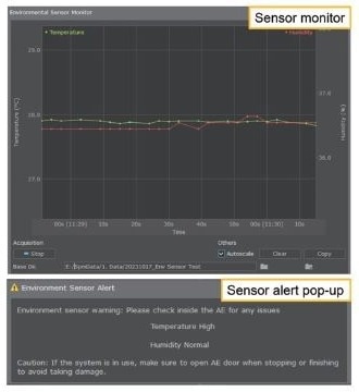
Figure 7. Captured SmartScan™ for environment monitoring. Changes in real-time temperature and humidity can be checked with plot charts, and if it is out of the designated range, the researcher is informed by alert pop-up. Image Credit: Park Systems
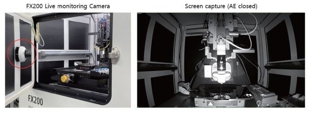
Figure 8. Live monitoring camera. A live monitoring camera enables real-time observation of the inside of AE. Image Credit: Park Systems
Conclusions
Innovations in AFM have transformed surface characterization in many scientific and industrial domains. Its distinctive capabilities continue to influence academic research and are increasingly integral to manufacturing and material analysis processes.
As the field progresses, AFM will play an even greater role in future discoveries and technological developments. Park Systems’ FX200 reflects a commitment to enabling the next generation of research with greater efficiency and ease.
By offering automated probe exchange and intelligent measurement processes, the FX200 delivers both exceptional convenience and dependable performance. With industry-leading Park AFM technology and advanced automation, the FX200 sets a new standard for high-precision AFM systems in shared laboratories and industrial settings.
This information has been sourced, reviewed and adapted from materials provided by Park Systems.
For more information on this source, please visit Park Systems.