Park AFM-IR combines nanoscale infrared (IR) spectroscopy and atomic force microscopy (AFM) to provide enhanced chemical and material characterisation. This system provides unprecedented performance in nanoscale research by combining the most recent infrared spectroscopy technology, photo-induced force microscopy (PiFM), into the industry-leading Park AFM platform.
Advanced Park AFM-IR Spectroscopy
High Spatial Resolution Chemical Imaging
While maintaining consistently high resolution and measurement accuracy throughout the investigation, Park AFM-IR provides spatial resolution that surpasses traditional IR spectroscopy and other nanoscale techniques. Reliable measurements are made possible by the non-contact method's avoidance of tip contamination and sample damage.
This capability takes molecular investigation into the nanoscale realm by offering chemical mapping and IR absorption spectra with a spatial resolution of about 10 nm and monolayer sensitivity. Direct drive and sideband bimodal detection approaches provide depth-sensitive insights, while including sideband techniques allows the detection of subtle molecular bonding information.
Automated IR Laser Beam Alignment
The FX series AFM systems are efficient, with automated probe mounting and IR laser alignment. This simplified setup drastically cuts down on measurement preparation time, improving user convenience overall.
Comprehensive Material Analysis
Park AFM-IR provides an integrated method for material characterization by simultaneously collecting high-resolution topography, IR spectra, and chemical mapping at specified wave numbers. It also includes more AFM-based measurements of mechanical, electrical, and thermal properties. This comprehensive capability is particularly useful in semiconductor research. The technology offers exact defect detection and nanoscale material composition identification, allowing for detailed failure analysis and device characterization.
Cutting-Edge PiFM Technology
In terms of spatial resolution, measurement dependability, and sample safety, the PiFM method uses a non-contact detection methodology that outperforms conventional techniques such as tapping PTIR (photothermal induced resonance). This preserves fragile samples while guaranteeing more accurate and reliable results. Users can acquire high-resolution infrared spectra and nanoscale images of infrared absorption with Park AFM-IR.
This capability allows for extensive chemical investigation of complicated materials. Furthermore, the high-resolution IR spectra exhibit a strong connection with traditional FTIR (Fourier Transform Infrared) spectroscopy. Advanced detection technologies, such as direct drive and sideband bimodal approaches, enable the retrieval of significant material information from various depths.
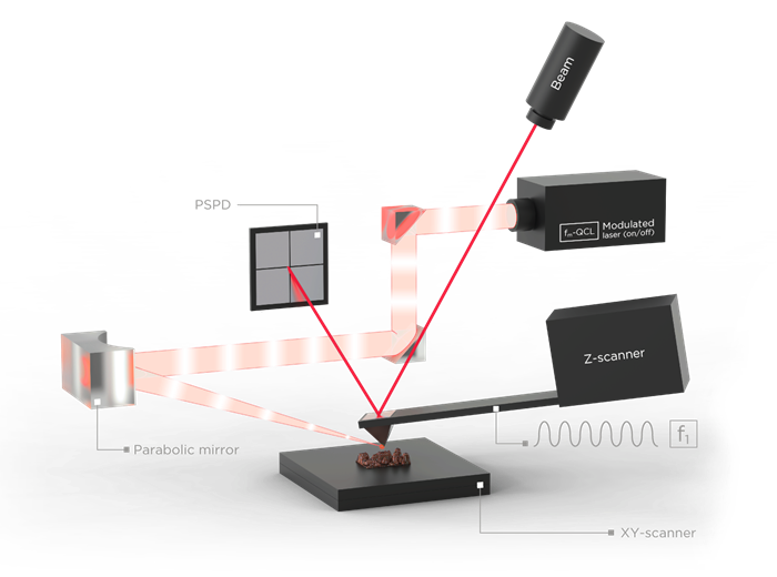
Image Credit: Park Systems
Key Features and Availability
Park AFM-IR is compatible with FX200 IR, FX300 IR, and FX300* systems and offers the following features:
- Flexible sample measurements for wafers ranging in size from small to 300 mm
- Automated IR Laser Beam Alignment for a streamlined measurement setup
- High-precision IR spectral measurement with PiFM, providing improved spatial resolution and robust FTIR comparability
- Advanced AFM applications include nanomechanical, electrical, and thermal property measurements
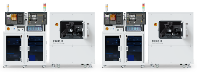
Image Credit: Park Systems