Park FX300 is intended to bridge the gap between research and industry applications, making it a true game changer in atomic force microscopy. It enables a variety of AFM techniques designed for research, quality control, and reliability assurance. The Park FX300 offers industry-specific research capabilities such as surface roughness assessment across wide areas and accurate wafer-level alignment and orientation control.
It also has improved optical setups for better sample visibility and contamination control for ultra-clean measuring conditions. These qualities make the Park FX300 an essential option for semiconductor post-processing, wafer-level packaging, and other cutting-edge industrial R&D applications.
Advanced Capabilities for Industrial & Research AFM Applications
300 mm Wafer Measurement Supporting Advanced Applications
It can measure up to 300 mm wafers and supports various advanced AFM applications, including the optional nano-IR technology.
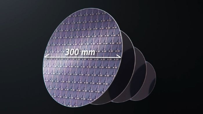
Image Credit: Park Systems
Specialized Industrial R&D Applications
Specialized industrial research and development applications feature long-range surface roughness profiling, recipe-based routine measurements, and a rotatable stage.
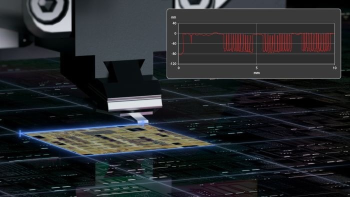
Image Credit: Park Systems
Enhanced Optical Sample Visualization
Sample visualization is improved with optional advanced off-axis optical setups.
Image Credit: Park Systems
Integrated Industrial-Grade Facility
Integrated industrial-grade facility with a facility controller, a signal tower with an emergency shut-off unit, and optional contamination control solutions utilizing a fan filter unit.
Image Credit: Park Systems
Intelligent Automation
It automates key tasks like probe recognition and exchange, laser alignment, and parameter tuning, significantly streamlining workflows. With 16 probe slots available, it supports repeated measurements and smooth mode transitions, minimizing downtime and enhancing overall productivity.
Automatic Probe Type Recognition
The Probe Identification Camera detects the QR code imprinted on the chip carrier of a new probe and displays all relevant information about each tip, such as kind, model, application, and usage. This enables the quick selection of the optimal probe tip for each work, assuring precision and efficiency.
Automatic Probe Exchange
Automated probe exchange allows for the easy and safe replacement of outdated probes. It has 16 probe slots for repetitive measurements and mode changes, eliminating downtime and enhancing efficiency by switching probes quickly and autonomously.
Automatic Laser Beam Alignment
Automatic Beam Alignment directs the laser beam to the appropriate cantilever point and optimizes the spot's vertical and lateral position on the PSPD. It autonomously shifts the X, Y, and Z axes for crisper, distortion-free images with the push of a button.
Simplified Operation
Automatic Sequential Measurement
Predefined coordinate settings can be applied to big samples, such as 300 mm wafers or samples on multi-sample chucks, for automated execution. It allows for sequential measurements, including topography and advanced modes, as well as the simplification of workflows in research and industrial applications.
Next-Generation AFM Controller for High-End Products
The Park FX Controller is specifically intended to improve the performance of the Park FX Series. This important advancement enables sophisticated Piezoresponse Force Microscopy (PFM) applications, including Contact Resonance PFM (CR-PFM) and Dual-Frequency Resonance Tracking (DFRT-PFM), without the need for extra hardware. This means that customers can fully benefit from the newest advances in atomic force microscopy.
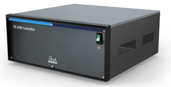
Image Credit: Park Systems
- DFRT-PFM without external amplifiers
- Direct CR-PFM enablement with improved bandwidth for tip bias modulation
- Improved safety and real-time assessment of the environment
- Faster Ethernet connectivity for efficient data and image processing
Park AFM-IR Spectroscopy
Advanced AFM-IR Spectroscopy for Large Sample Chemical Analysis
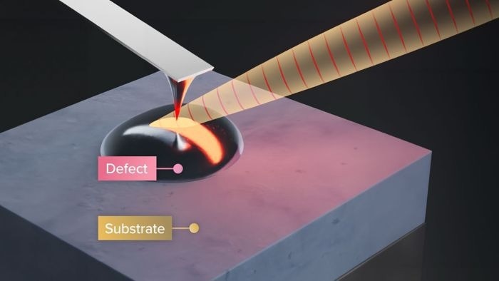
Image Credit: Park Systems
Park AFM-IR is a combined infrared (IR) spectroscopy and atomic force microscopy (AFM) instrument. The spectroscopic section identifies chemical compounds with a spatial resolution of 5 nm.
It employs a non-contact approach providing the safest spectrum scanning and industry-leading spatial resolution. The microscopy component displays nanoscale 3D topography with sub-angstrom height accuracy as well as mechanical property information to the user.