Sponsored by Park SystemsReviewed by Olivia FrostJun 13 2025
With the advancement of nanotechnology, understanding surface properties at the nano- and sub-nanoscale has become increasingly important. Characteristics such as topography and roughness play a critical role in determining the overall performance of a material.

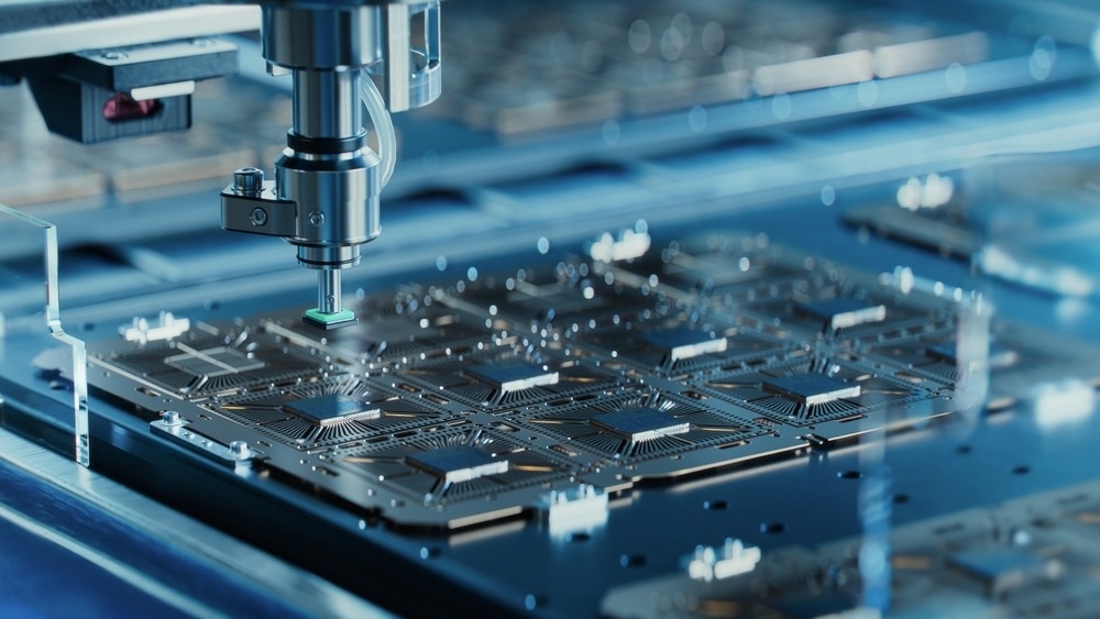
Image Credit: IM Imagery/Shutterstock.com
For instance, in integrated circuit manufacturing, chemical mechanical polishing (CMP) is commonly employed to control surface roughness of wafers and other substrates - an essential factor in ensuring product reliability.1,2
In semiconductor device packaging, the quality of wafer-to-wafer bonding is directly influenced by the roughness of the bonding surfaces. Studies have shown that high surface roughness can introduce voids at the bonded interface, with bonding failures occurring when roughness exceeds a critical threshold.3
In broader scientific research, surface topography is often correlated with other material properties to better understand behavior under practical conditions.4-6
To characterize surface topography, several techniques are available, including stylus profilometry, coherence scanning interferometry, laser microscopy, and atomic force microscopy (AFM). The selection of a method depends on the sample’s characteristics and the specific measurement objectives.
In semiconductor and electronic device manufacturing, where detailed insights into nanoscale surface features are essential, AFM has emerged as a widely adopted technique. Its ability to provide three-dimensional data at sub-nanometer resolution makes it particularly well suited for such applications.
Moreover, the scanning probe-based approach of AFM enables simultaneous measurements of surface topography along with various electrical, frictional, and mechanical properties, thereby improving both efficiency and throughput.
Measuring Surface Properties Using AFM
AFM has been widely adopted by both industrial chip manufacturers and academic researchers for nanoscale surface measurements across a variety of materials. AFM can be applied in both in-line and off-line modes for quality control and inspection throughout semiconductor and display manufacturing processes.
Common applications include surface roughness inspection of bare wafers,7 post-CMP roughness measurement,1,2 monitoring of wafer bonding processes,3,8 and defect inspection and review in hard disk media.7
In academic research, AFM is frequently used for surface measurements related to nanomaterials,8 studies that correlate surface characteristics with other material properties,4 and investigations into how environmental factors influence surface behavior.5,6
Since AFM operates by scanning the sample surface with a nanoscopic tip, understanding the interaction between the tip and the sample is critical for accurate data analysis and interpretation.
This article will review AFM methodologies commonly used to investigate sample topography and surface roughness. Particular attention is given to AFM data analysis and interpretation procedures, along with experimental considerations necessary for accurate surface reconstruction.

 Download the full article now to read on.
References
- Zhao, D. and Lu, X. (2013). Chemical mechanical polishing: Theory and experiment. Friction, 1(4), pp.306–326. https://doi.org/10.1007/s40544-013-0035-x.
- Xie, W., et al. (2020). Green chemical mechanical polishing of sapphire wafers using a novel slurry. 12(44), pp.22518–22526. https://doi.org/10.1039/d0nr04705h.
- Chen, G., et al. (1999). The effect of surface roughness on direct wafer bonding. Journal of Applied Physics, 85(10), pp.7448–7454. https://doi.org/10.1063/1.369377.
- Mario, Carlos, Lanzoni, E.M., et al. (2019). Unraveling the Role of Sn Segregation in the Electronic Transport of Polycrystalline Hematite: Raising the Electronic Conductivity by Lowering the Grain-Boundary Blocking Effect. Advanced Electronic Materials, 5(6). https://doi.org/10.1002/aelm.201900065.
- Salomão, F.C., et al. (2015). Determination of High-Frequency Dielectric Constant and Surface Potential of Graphene Oxide and Influence of Humidity by Kelvin Probe Force Microscopy. Langmuir, 31(41), pp.11339–11343. https://doi.org/10.1021/acs.langmuir.5b01786.
- Song, H., et al. (2020). Influence of humidity for preparing sol-gel ZnO layer: Characterization and optimization for optoelectronic device applications. Applied Surface Science, (online) 512, p.145660. https://doi.org/10.1016/j.apsusc.2020.145660.
- Yoo, R.Y. (2014). Automated AFM Boosts Throughput in Automatic Defect Review. Microscopy Today, 22(6), pp.18–23. https://doi.org/10.1017/s1551929514001126.
- Nagano, F., et al. (2022). Void Formation Mechanism Related to Particles During Wafer-to-Wafer Direct Bonding. ECS Journal of Solid State Science and Technology, 11(6), p.063012. https://doi.org/10.1149/2162-8777/ac7662.

This information has been sourced, reviewed and adapted from materials provided by Park Systems.
For more information on this source, please visit Park Systems.