Wide bandgap semiconductor materials are highly useful in power electronics due to their ability to work at high temperatures, power, and frequency.
Gallium nitride (GaN) is a wide bandgap semiconductor used in power device manufacturing because it outperforms silicon high-voltage devices and is less expensive than silicon carbide (SiC) power devices.
The features of GaN high-electron mobility transistor (HEMT) devices on a SiC substrate have been tuned for high-temperature electronics, radio frequency (RF) power amplifiers, and power microwave applications.
The GaN/SiC HEMT manufacturing flow typically includes the following steps: SiC substrate formation, GaN epitaxy, etch, front-side device development, wafer bonding to carrier, wafer thinning, hard mask fabrication, via-hole etching, Au electroplating, wafer debonding/cleaning, packaging, via-hole etching process, and Au electroplating.
Figure 1 shows the backside via structure before (top) and after (bottom) the Au electroplating process. Monitoring the via etch process is crucial since etch quality directly impacts the performance of HEMT devices. This step's critical metrology characteristics are the opening diameter and average depth of the via holes.
Scanning electron microscopes (SEMs) can determine hole depth in high aspect ratio (~1:3) structures; however, they are damaging and have low throughput. In contrast, 3D optical profiling provides a nondestructive, high-throughput method of evaluating key dimensions in vias.
The KLA Instruments™ Zeta™ optical profilers offer 3D imaging and metrology in a cost-effective, versatile design. The combination of White Light Interferometry (WLI) and Zeta's unique ZDot™ technology offers speedy and quantitative surface analysis for off-line product evaluation.
The Zeta software includes recipes for via hole applications that automatically collect data on depth, opening size, and bottom roughness from numerous sites. It is a dependable and effective way to monitor and optimize HEMT vias.
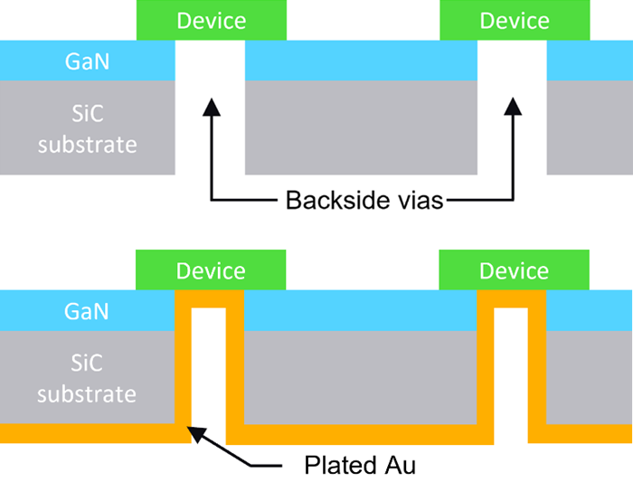
Figure 1. GaN/SiC HEMT backside via structure (top) and Au-plated GaN/SiC HEMT backside via structure (bottom). Image Credit: KLA Instruments™
WLI Theory of Operation
The Zeta optical profiler is a fully integrated microscope-based system that employs WLI (Vertical Scanning Interferometry, or VSI) and other optical techniques to enable non-contact 3D imaging and metrology. Figure 2 (top) shows the WLI objective schematic.
The interferometer objective is mounted on a piezoelectric transducer (PZT) or a motorized stage and can be moved vertically.
The reference mirror is utilized in conjunction with the white LED light source, and the distance between the objective lens and the reference focus plane surface remains constant during the vertical scanning action.
The interference of light reflected from the reference mirror with the sample surface produces fringes utilized to evaluate sample geometries. Based on these fringes, the white light generates the contrast peak location of each CCD camera pixel, which is represented by its z position in Figure 2.
After scanning vertically, the software recognizes the z information to generate a 3D topographic image, which can subsequently be utilized to determine dimensions and step height information. In addition, the WLI approach can measure the topography of flat surfaces with excellent z resolution.
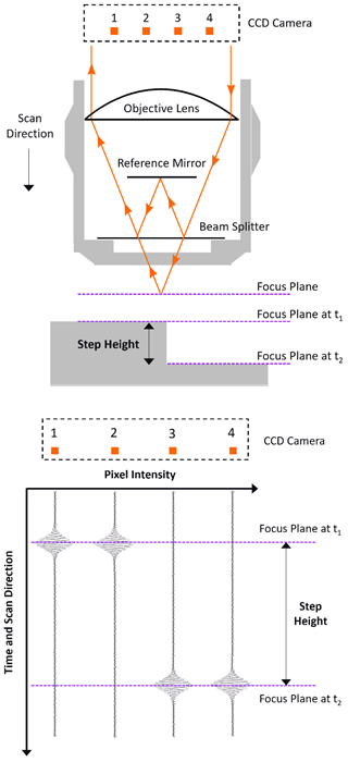
Figure 2. White Light Interferometry (WLI) schematic. The top figure shows the reference mirror and light paths of a Mirau interferometer objective. The bottom figure shows the intensity of each CCD camera pixel, which is maximized when the sample surface is in focus. Image Credit: KLA Instruments™
ZDot™ Theory of Operations
The KLA Instruments Zeta optical profilers include unique ZDot technology in the same optics system. Figure 3 shows ZDot's utilization of two high-intensity white LED light sources.
Light from source 1 travels across the ZDot grid, generating each pixel's contrast peak location as its z position, whilst light from source 2 preserves the True Color imaging information at each pixel.
ZDot technology offers precise assessment of a wide range of sample topographies while also producing a 3D True Color image.
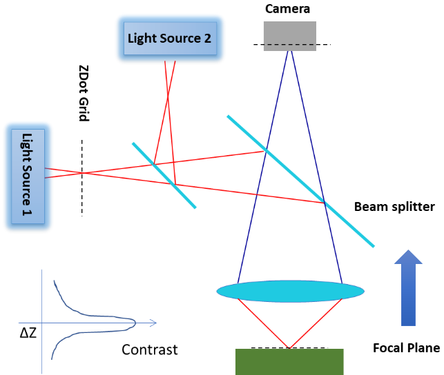
Figure 3. ZDot technology schematic. Image Credit: KLA Instruments™
Measurement of High Aspect Ratio Vias
3D optical profiling is useful because it allows non-destructive measurement of small apertures and deep vias in high aspect ratio structures, which are usually difficult to measure using non-optical measuring metrology.
Low numerical aperture (NA) objectives are suggested for these types of high-aspect ratio measurements because they have a lower percentage of blocked angles of reflected light than high NA objectives, as illustrated in Figure 4.
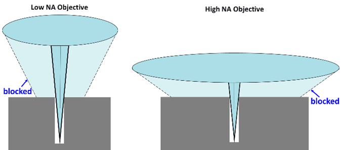
Figure 4. The reflected light in a deep hole is shown for low NA (left) and high NA (right) objectives. The low NA objective has less light blocked than the high NA objective, resulting in a greater reflected signal. Image Credit: KLA Instruments™
A low NA objective allows more light intensity to reach the camera from the bottom surface of the via, resulting in better imaging quality while measuring deep features. The Zeta optical profiler uses low NA and WLI technology with vertical scanning to measure square vias with opening sizes of 30 µm x 30 µm and depths of 90 - 110 µm.
The Zeta program includes powerful automatic analysis methods for characterizing high aspect ratio HEMT vias that employ WLI technology. Figure 5 shows the measured two-dimensional cross-section of an HEMT via.
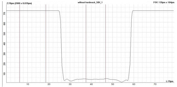
Figure 5. 2D profile from a 3D HEMT via scan, showing the via cross-section and depth measurement. Image Credit: KLA Instruments™
The Zeta optical profiler's 2D profile can also measure tapered sidewalls. During the etch process, the via sidewalls are often vertical; reflected ions generate a localized increase in the ion flux near the bottom of the feature, increasing etch rate.
Improved etch process parameters, such as plasma pressure, chemistry, and bias, can significantly lower the sidewall taper. Figure 6 shows an SEM picture with tapered sidewalls. Sidewall taper must be considered while developing robust hole metrology recipes.
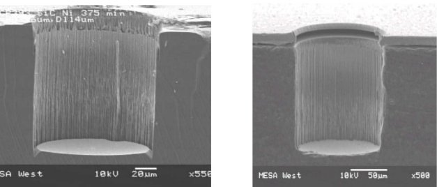
Figure 6. Vias as imaged by SEM. Image Credit: KLA Instruments™
The Zeta software can automatically detect via holes and set measurement cursor points. This feature identification technique provides three ways for detecting certain features using picture RGB information, pixel intensity, and height. A via is analyzed using the height information from the 3D measurement.
The software detects hole characteristics in the field of view and labels the centers with a red cross and the edges with a red line, as shown in Figure 7.
In this example, the recipe creates a blue box within the red box by reducing the number of measuring pixels perpendicular to the surrounding red contour, avoiding the impact of sidewall slope and bottom shape induced by the etch process on measurement results.
A user-defined reference box is displayed in the upper left corner of the image, and the average depth is calculated as the height difference between the reference box and the blue box.
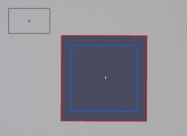
Figure 7. Top-down True Color image of a square hole, where the software automatically defines the feature edges in red. The hole depth is calculated as the difference between the reference z height (gray box at upper left) and the bottom surface z height (blue box at center). Image Credit: KLA Instruments™
The analysis results contain the following parameters, as shown in Figure 8:
- MajorAxis is the structure's long axis diameter, measured in microns using the red box border lateral dimensions.
- MinorAxis is the structure's short axis diameter measured in microns based on the red box boundary lateral dimensions.
- AvgDia is the average of the long axis and short axis diameters, in microns; this value is used to calculate the top opening size for openings that are not strictly circular. Data is based on the red box boundaries.
- Sa is the areal surface roughness, measured in microns based on blue box boundaries.
- AvgHeight is the average depth in microns relative to the reference surface height, based on grey and blue box boundaries.
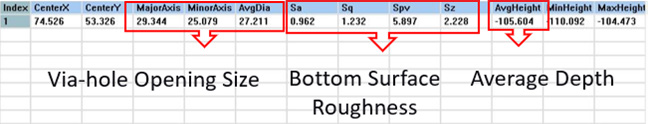
Figure 8. Data report from the Zeta optical profiler displays the measurement results, including hole diameter, roughness of bottom surface, and average depth. Image Credit: KLA Instruments™
The reporting area displays all parameters and allows you to export them as *.txt or *.csv files. For higher volume production measurement applications, these parameters can be automatically exported to a remote host via SECS/GEM with the Zeta-388 fully-automated optical profiler.
Measurement of Obround/Elliptical Vias
HEMT vias come in a variety of shapes, including circular, square, elliptical, and obround (also known as stadium or racetrack). Figure 9 shows a top-down picture of the surrounding HEMT structures.
The vias are 75 µm × 35 µm and range in depth from 90 to 110 µm. The Zeta optical profiler uses the WLI technique in conjunction with advanced automatic analytic algorithms to measure and report on characteristics such as Depth, Bottom Roughness, MajorAxis, and MinorAxis.
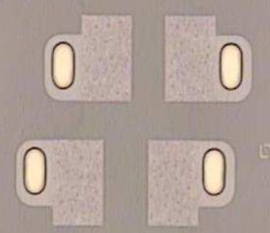
Figure 9. Obround HEMT vias measured by the Zeta optical profiler. Image Credit: KLA Instruments™
Measurement of Hard Mask Openings
Etching the hard mask opening is the initial step in creating the via hole structure on SiC and GaN substrates. The size of the hard mask opening is an important characteristic to monitor since it influences subsequent etch procedures.
Due to the extremely rough surface, the usage of WLI technology may be limited in this application. As previously stated, the reference mirror will produce fringes when the surface is in focus. However, steep slopes make it harder to create fringes from rough surfaces, resulting in an increased number of non-measurable pixels.
Non-measured pixels have an impact on measurement results because signal information is lost in high slope locations. The Zeta optical profiler with ZDot technology enhances WLI measurements by precisely measuring the 3D image on the rough hard mask surface.
ZDot can identify and report all metrics from 3D hard mask opening measurements, including depth, bottom roughness, and diameter opening size. Figure 10 shows a 3D True Color image and example line profile of a rough surface measured with ZDot technology.
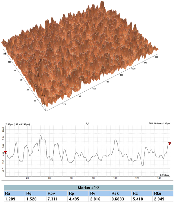
Figure 10. Top: 3D image of a rough surface measurement taken using ZDot technology. Bottom: 2D profile across the surface with measured ISO roughness parameters. All dimensions are microns. Image Credit: KLA Instruments™
Conclusions
The Zeta optical profiler uses non-destructive and high-throughput metrology techniques to accurately measure and automate the examination of high-aspect-ratio structures such as HEMT vias. The Zeta's multi-function design allows for the selection and tuning of the most appropriate metrology mode for the type of sample being measured.
KLA Instruments' Zeta optical profilers are designed for optimum application flexibility. The Zeta tools' Multi-Mode capability enables ZDot and True Color imaging, phase and vertical scanning interferometry, interference contrast imaging, shearing interferometry, film thickness and reflectance measurement, and defect detection and mapping.

This information has been sourced, reviewed and adapted from materials provided by KLA Instruments™.
For more information on this source, please visit KLA Instruments™.