Sheet resistance monitoring is essential for ion implant doping and anneal characterization. It’s also commonly used in processes such as ion implantation, metal deposition, diffusion, and epitaxial silicon growth to support development, monitoring, and control. The Four-Point Probe (4PP) technique remains the most widely used method due to its simplicity and accuracy.
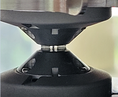
Image Credit: KLA Instruments™
The latest in over 45 years of KLA's resistivity measurement technology, the KLA Instruments™ R54-Series offers benchtop sheet resistance mapping systems. The R54-4PP series is light-tight, production-ready, and part of the KLA Instruments™ Sheet Resistance product line.
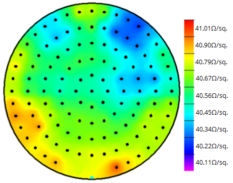
Figure 1. Sheet resistance map of an As-doped substrate; this high density, high uniformity contour map provides a quality check on the deposition process, where the required uniformity is < 0.5 %. The accuracy and repeatability of the R54 delivers the performance required for monitoring the sensitive doping process. Image Credit: KLA Instruments™
Four-Point Probe Measurement Technique
The four-point probe technique is an established technology that has been used to monitor the implant process for many years.
Figure 2 shows a linear array four-point probe design in which electrical current is transmitted between two pins in contact with a conductive surface while voltage is monitored between two additional pins in contact with the surface.
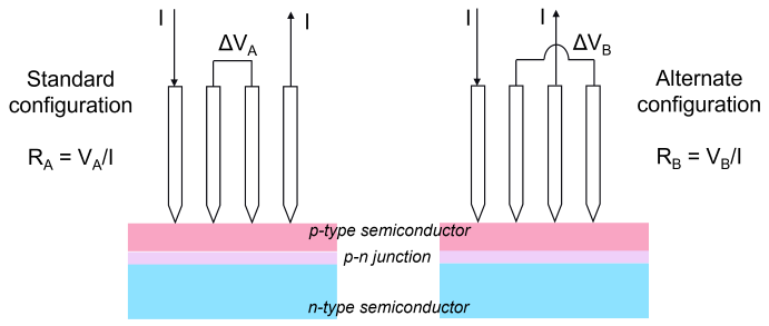
Figure 2. Four-point probe pin schematic for the Dual Configuration measurement method, which is typically used in cases of current crowding at the edge of a film or when pin spacing variation requires correction. Image Credit: KLA Instruments™
The four-point probe requires an isolating junction or blocking layer to protect the DC current employed in this technique. The ion implant procedure uses a p-n junction. A p-n junction is often produced between an ion implantation layer and the substrate.
This connection is near to the surface in an ultra-thin implant layer and may necessitate particular precautions to reduce probe penetration. To create the connection and activate the ions, an anneal is necessary before four-point probe measurements, which can be performed on the implant monitor wafer.
Implant Process Shifts
4PP contour maps of sheet resistance (Rs) can assist in spotting ion implant process shifts, such as greater Rs due to significant thermal loss, where an anneal process may not achieve the needed temperature to fully activate the ions in the ion implant layer.
Another concern is "hot spots" on the wafer, which, due to locally elevated temperatures, result in increased ion activation and drive down the junction, as illustrated in Figure 3.
4PP uniformity mapping can also help troubleshoot a lamp array in which a lamp has degenerated or failed. This problem causes outside edge cool areas to have poor coupling with the platen, which can be identified by the increased relative sheet resistance.
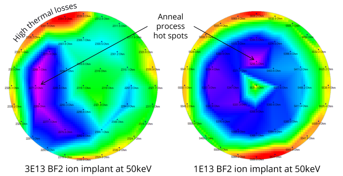
Figure 3. Identifying hot and cold spots is critical to detecting and resolving lamp failures and poor wafer/platen contact, which lead to semiconductor device failure. Image Credit: KLA Instruments™
Laser Annealing Characterization
As previously stated, the annealing procedure is employed to activate the implanted ions. A laser anneal melts the silicon in a small region on the wafer's surface, activating the ions as it recrystallizes.
Figure 4 shows a graph of sheet resistance as a function of radial position, with the sawtooth (stitching) pattern of high-to-low sheet resistance indicating that the laser beam's width is excessively small in comparison to the scan pattern across the wafer's surface.
This issue can only be identified with a high-density 4PP measuring pattern and a very reproducible 4PP signal with a high signal-to-noise ratio, such as the R54.
If the laser beam diameter and scanning patterns are not properly set, a resistance "ripple" is formed, causing cross-die resistance fluctuation and poor device performance.
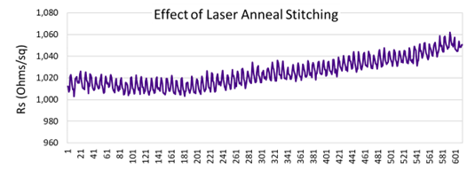
Figure 4. This 600-site diameter sheet resistance scan exposes an issue with a laser anneal of ion-implanted silicon by revealing the periodic variation caused by the laser beam width. Image Credit: KLA Instruments™
Short-term lateral variations are best detected using high-density maps or line scans across the target area. Probes with narrow pin spacing enhance lateral resolution; for example, a 0.65 mm pin spacing provides an effective measurement spot size of less than 1 mm.
Four-Point Probe Performance
To ensure probe performance on implant wafers, repeatability tests are used to quantify system performance.
Four-point probe performance is affected by several factors, including proper sample preparation and selecting the appropriate probe head (the R54 supports a range of probe head types depending on the application). It is important to eliminate these potential error sources so they do not contribute to measurement uncertainty.
With careful preparation of implant monitor samples and a properly conditioned probe head, it is expected that reliable performance is achievable for ion implant doses down to 1E12 ions/cm2.
Probe qualification exams are widely used to assess 4PP performance. Each probe should be conditioned until it meets the specified qualifying value (usually < 0.2%).
Achieving < 0.2% accuracy demands careful attention to the pin tip's ohmic contact with the sample, yet it leads to high-quality measurements of multiple implant layers. For very shallow implant layers, increasing the tip contact area often improves repeatability.
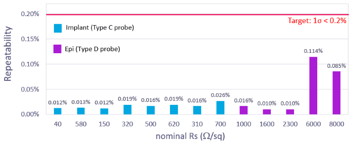
Figure 5. It is important to use the proper probe with sufficient conditioning to produce probe qualification standard deviations of < 0.2 % on the R54-200. Image Credit: KLA Instruments™
I-V Curve Plotting
The vertical distance from the wafer surface to the depth at which the embedded dopant type changes to that of the background dopant type is defined as the junction depth. In some cases, higher current may penetrate through the implanted layer and leak through the junction barrier.
By monitoring the voltage or sheet resistance (Rs) response curves, issues such as low signal-to-noise current, joule heating, or junction breakdown can be avoided.
The KLA Instruments Filmetrics R54 RsMapper software includes additional functionality for implant characterization by plotting sheet resistance or measured voltage as a function of applied current, as shown in Figure 6. This feature provides verification of the linearity of the pin contacts and the stability of Rs, helping ensure that an appropriate current has been selected.
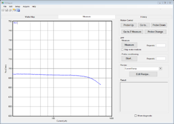
Figure 6. The RsMapper software for the R54 can be configured to run a current ramp routine to ensure that the appropriate current is selected for measurement, targeting optimal signal to noise and avoiding regions of current leakage. This dataset indicates current leakage above 100 mA. Image Credit: KLA Instruments™
Conclusion
By combining probe qualification tests with I-V curve monitoring, R54 users with light-sensitive samples can have confidence in the accuracy of their implant characterization on monitor wafers.
The Filmetrics R54-series provides dependable data acquisition and analysis features, serving a crucial purpose for semiconductor metrology by identifying equipment performance fluctuation at various phases of the ion implant process.

This information has been sourced, reviewed and adapted from materials provided by KLA Instruments™.
For more information on this source, please visit KLA Instruments™.