Sponsored by Vitrek, LLCReviewed by Maria OsipovaSep 18 2025
Wafer lapping is a vital semiconductor thinning operation that requires precise control to avoid over-removal of material, which can result in significant yield loss.
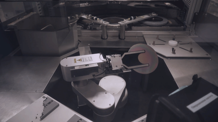
Image Credit: Vitrek, LLC
This article explains how MTI Instruments' Accumeasure™ capacitive sensing technology provided precise, real-time displacement and thickness measurement during lapping processes, resulting in consistent wafer quality.
Challenge
During lapping, a spinning abrasive surface is used to thin wafers from the backside. As the process progresses, precise feedback is required to monitor the amount of material removed and determine the wafer's final thickness.
Traditional mechanical or visual checks are insufficiently sensitive or rapid for today's semiconductor manufacturing tolerances.
The Solution: MTI’s Non-Contact Capacitance-Based Measurement System
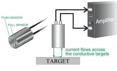
Image Credit: Vitrek, LLC
MTI's Accumeasure™ high-resolution device monitors displacement with sub-micron accuracy, even in electrically loud rotating lapping environments.
Lapping System Overview
- A semiconductor wafer was sandwiched between a Pyrex plate and fluid barrier above the spinning lapping wheel.
- Simulated production conditions by applying continual downward pressure with a metal weight.
- MTI's capacitance sensor was located above the floating weight, which was not grounded.
- A second probe monitored the vertical displacement of the lapping plate.
As the wafer thinned, the metal weight gradually decreased. The relative displacement of the weight and the lapping plate is directly related to the material removed from the wafer.
Why Push-Pull Probes?
MTI's push-pull probes provide extremely accurate displacement measurements, even when the target is ungrounded or spinning. Instead of single-ended probes, push-pull designs use twin, out-of-phase signals that flow across the target surface, eliminating grounding mistakes and noise interference.
This makes them ideal for dynamic environments where accurate, high-resolution data is required for process management.
Data Acquisition and Signal Processing
Data from both probes is digitized by MTI's amplifier and examined with LabVIEW software. Key steps included:
- Anti-alias filtering with a 5 kHz cutoff and a sampling rate of 20 kSPS.
- Extract median signal to eliminate spikes caused by grooves on the lapping plate.
- Auto-zeroing at process start establishes a thickness baseline.
- Real-time monitoring of the distance between the weight and plate.
Custom LabVIEW methods use boxcar averaging and sample-based median filtering to smooth out groove noise and surface imperfections.
Push-Pull Probe Key Advantages
MTI push-pull probes offer:
- High Accuracy — Ideal for ungrounded or floating targets, like the rotating weight.
- Eliminate Measurement Errors — The signal is driven across the surface, not through the part.
Probes deliver:
- 2 mm measurement range
- 0.2 µm resolution
- Robust performance in dynamic lapping environments
Results: Accurate, Real-Time Wafer Thickness Calculation
Customers can use MTI's Accumeasure technology to ensure accurate, real-time wafer thickness monitoring during the lapping process. By continuously measuring the distance between the lapping weight and the plate, the system estimates the amount of material removed with precision.
The original wafer thickness was compared to the measured loss to get the current thickness at any given time.
When the required thinning was reached, automated alerts triggered the operation to cease before overlapping began. This strategy greatly improved process uniformity, reduced scrap, and increased total yield.
System Benefits
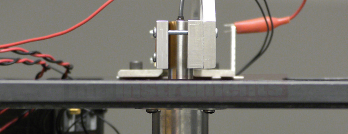
Image Credit: Vitrek, LLC
- Non-contact, high-precision thickness tracking
- Real-time feedback for process control
- Dependable in electrically isolated or noisy situations
- Automated notifications to prevent overlapping
Conclusion
This semiconductor customer was able to retain tight control over wafer thinning using MTI's Accumeasure technology, which provided unrivaled precision and automated process feedback. The end result was higher yield, throughput, and quality control in a critical fabrication phase.

This information has been sourced, reviewed and adapted from materials provided by Vitrek, LLC.
For more information on this source, please visit Vitrek, LLC.