Sponsored by Vitrek, LLCReviewed by Maria OsipovaOct 9 2025
The wafer lapping process is key to effective semiconductor thinning. It requires extremely tight control to avoid over-removal of material and the resulting expensive yield loss.
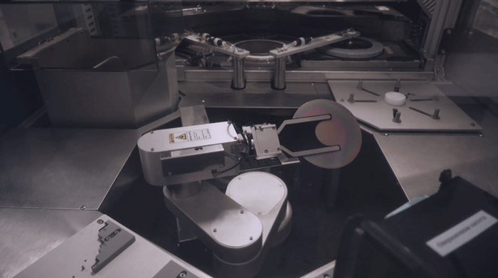
Image Credit: Vitrek, LLC
This article examines the role of MTI Instruments’ Accumeasure™ capacitive sensing technology in ensuring consistent wafer quality. This technology is designed to facilitate precise, real-time displacement and thickness measurement during lapping operations.
Challenge
The lapping process involves thinning wafers from the back with a rotating abrasive surface. It is important to receive precise feedback as the process is carried out to monitor the quantity of material removed and determine the final thickness of the wafer.
With today’s semiconductor manufacturing tolerances, visual inspections or conventional mechanical methods are just not fast or sensitive enough.
The Solution: MTI’s Non-Contact Capacitance-Based Measurement System
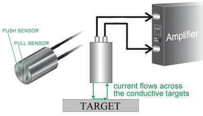
Image Credit: Vitrek, LLC
MTI's Accumeasure™ is a powerful, high-resolution system that uses push-pull capacitance probes to monitor displacement with sub-micron accuracy. This level of accuracy is even possible in a rotating lapping environment, despite it typically having high electrical noise levels.
Lapping System Overview
The lapping system involved sandwiching a semiconductor wafer between a Pyrex plate and a fluid barrier above the rotating lapping wheel.
A metal weight was used to apply constant downward pressure to simulate production conditions.
The weight was electrically ungrounded and placed below the mounted MTI's push-pull capacitance probe. A second probe was used to track the lapping plate’s vertical displacement.
The metal weight gradually dropped as the wafer thinned, with the relative displacement between the weight and lapping plate directly corresponding to material removed from the wafer.
Advantages of Push-Pull Probes
MTI’s push-pull probes ensure the collection of highly accurate displacement measurements, even in applications where the target is rotating or ungrounded.
Push-pull designs differ from single-ended probes as they use dual, out-of-phase signals that flow across the target surface. This approach eliminates noise interference and grounding errors, making push-pull probes ideally suited for use in dynamic environments where consistent, high-resolution data is required for effective process control.
MTI push-pull probes offer a range of benefits, including:
- High accuracy, making them ideal for use with ungrounded or floating targets, such as the rotating weight described.
- The elimination of measurement errors because the signal is driven across the surface rather than through the part.
- A two millimeter measurement range with 0.2 µm resolution
- Reliable performance, even in dynamic lapping environments
Data Acquisition and Signal Processing
With data acquisition and signal processing, the data is first digitized using MTI’s amplifier and analyzed with LabVIEW software. Key steps in this process include:
- Anti-alias filtering (five kHz cutoff) with a 20 kSPS sampling rate
- Median signal extraction to reject groove-induced spikes on the lapping plate
- Auto-zeroing at the start of the process to establish a thickness baseline
- Real-time monitoring of the gap change between the weight and the plate
- Smoothing groove noise and surface irregularities via custom LabVIEW routines with sample-based median filtering and boxcar averaging
Benefits of this system and approach include:
- High-precision, non-contact thickness tracking
- Real-time process control feedback
- Reliability in noisy or electrically isolated environments
- Automated alerts are designed to prevent overlapping
Results: Accurate, Real-Time Wafer Thickness Calculation
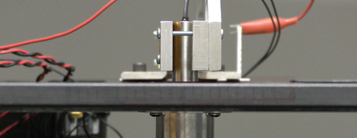
Image Credit: Vitrek, LLC
MTI’s Accumeasure™ system empowers its users to achieve accurate, real-time monitoring of wafer thickness throughout the wafer lapping process. Its ability to continuously measure displacement between the lapping weight and plate allows the system to precisely calculate the quantity of material removed.
Initial wafer thickness can be compared to the measured loss to determine the current thickness as required, and automated alarms signa when the desired thinning is achieved.
This technique ensures that the process is stopped before overlapping occurs, which significantly improves process consistency, reduces scrap, and improves overall yield.
Conclusion
MTI’s Accumeasure™ system allowed the semiconductor manufacturer in this example to maintain tight control over wafer thinning with automated process feedback and unparalleled precision. This ultimately led to improved yield, enhanced throughput, and more stringent quality control in this essential fabrication step.
Acknowledgments
Produced from materials originally authored by Vitrek.

This information has been sourced, reviewed, and adapted from materials provided by Vitrek, LLC.
For more information on this source, please visit Vitrek, LLC.