In this interview, AZoMaterials speaks with Fernando Castro, Application Scientist at Gatan, about the latest advancements in 4D STEM orientation mapping using the newly released STEMx OIM software within DigitalMicrograph. Fernando discusses how this tool simplifies orientation and phase mapping workflows while enabling high-resolution and multimodal analysis of nanoscale materials.
Can you please introduce yourself and your role at Gatan?
My name is Fernando Castro, and I’m an Application Scientist at Gatan. I support TEM imaging, diffraction and 4D STEM products like STEMx® and STEMx OIM.
My work involves both product development and customer training, with a recent focus on 4D STEM and orientation mapping areas. I hold a PhD in Materials Science and Engineering from Northwestern University, and I’ve been with Gatan since graduating in 2018.
What is STEMx OIM, and how does it enhance 4D STEM orientation mapping in DigitalMicrograph?
STEMx OIM is a new feature set within DigitalMicrograph® that enables automated orientation and phase mapping of your 4D STEM data, with no scripting needed. It uses a template matching algorithm to index diffraction patterns at each pixel and works for single or multiphase materials. This lets you acquire and calculate high-resolution orientation maps from your 4D STEM data while being incredibly user-friendly.
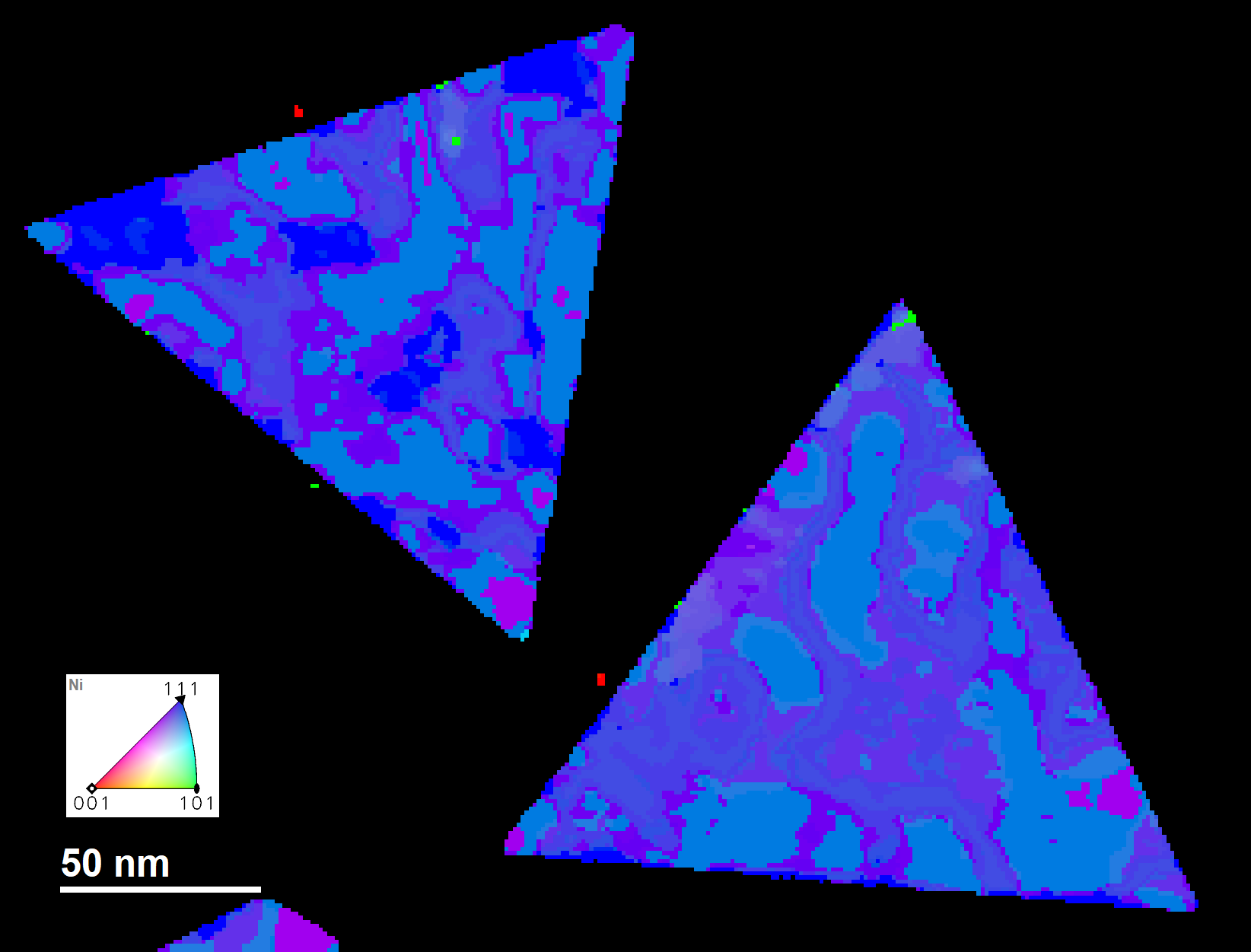
High-resolution orientation map of Ni platelets calculated with STEMx OIM (sample fabricated by Felipe Quiroga-Suavita, LPCNO - INSA Toulouse and SMS - UNSW Sydney, EU MSCA-AUFRANDE)
Why is orientation mapping important in electron microscopy, and how does 4D STEM compare to EBSD?
Orientation mapping lets us investigate grain structures, phase distributions, and grain boundaries; these are key factors for understanding material performance. While EBSD in the SEM is great for micrometer-scale mapping, STEM techniques like 4D STEM offer much higher spatial resolution, so it's ideal for nanoscale materials. There is also a difference in indexing algorithms, since EBSD indexes Kikuchi patterns and for 4D STEM we must index spot patterns.
How does STEMx OIM handle multiphase materials?
The workflow is straightforward: For each expected phase, you import a crystal structure file in *. CIF format. You can download structure files from online databases or use a structure in the included library. STEMx OIM then generates simulated diffraction patterns for the template matching algorithm and finds the best match pattern, orientation, and phase at each pixel position. If you have multiple phases, it will find the best match at each pixel across orientations of every phase you’ve chosen. It generates orientation maps and phase maps, and you can manually inspect the matching quality using heat maps to assess fit confidence.
What acquisition parameters are critical for successful orientation mapping?
Good 4D STEM data for orientation mapping will have high signal-to-noise and sharp diffraction spots. The size of the diffraction spot is controlled by the microscope convergence angle, with a smaller convergence angle giving sharper spots instead of larger diffraction discs. In one test, switching from a 2.5 mrad to a 0.7 mrad convergence angle significantly improved indexing results. Having high signal-to-noise ratios can be accomplished by optimizing the probe current and pixel time used for data collection, in addition to having a sensitive high-speed camera. Energy filtering can also benefit the 4D STEM data, as it will reduce the inelastic scattering background and improve signal-to-noise in your dataset.
Can 4D STEM orientation mapping be combined with other data, like EDS or EELS?
Absolutely. One major strength of using STEMx OIM is its integration in DigitalMicrograph, which unlocks multimodal analysis via eaSI technology. The acquisition tools in DigitalMicrograph enable you to acquire 4D STEM data simultaneously with EDS or sequentially with EELS. For example, we simultaneously acquired 4D STEM and EDS data from a multilayer, multielement sample and used the EDS data to identify specific compositional layers for orientation mapping. Similarly, combining EELS with 4D STEM enabled us to look at a cobalt oxide sample and understand both particle orientation and chemical variations in cobalt.
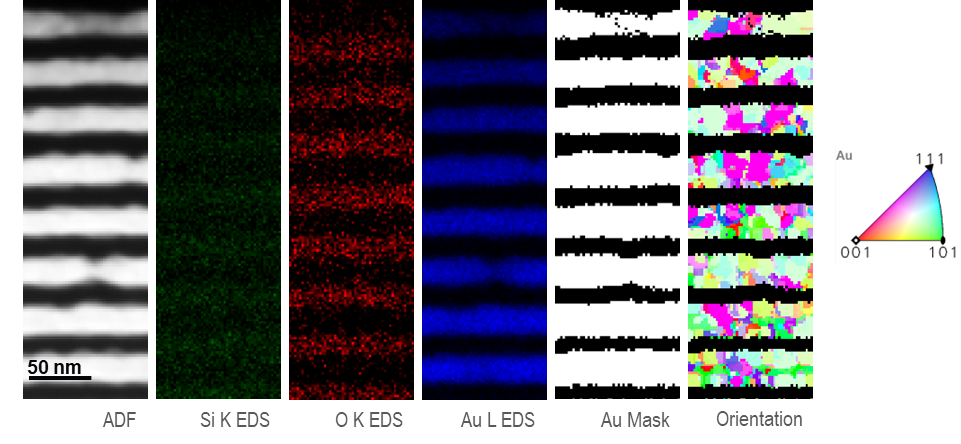
Multimodal analysis of SiO2/Au multilayer film. 4D STEM and EDS data were simultaneously acquired, and the Au EDS map was used for isolating the Au layers for orientation mapping with STEMx OIM.
Is STEMx OIM compatible with EBSD workflows and software?
Yes. You can calculate orientation maps with STEMx OIM and then export the maps to the EDAX® OIM Analysis™ software. As a result, users can use many more familiar EBSD tools on their data like twin boundary detection, grain size filtering, or pole figure analysis. This bridges the gap between traditional SEM-based EBSD and high-resolution TEM-based 4D STEM workflows.
What is STEMx Precession, and how does it benefit 4D STEM analysis?
STEMx Precession is a DigitalMicrograph feature under development that uses a sequential beam-tilt approach to acquire precessed 4D STEM datasets. This method enhances 4D STEM data quality by increasing diffraction spot uniformity, reducing dynamical scattering effects, and acquiring higher-order diffraction spots. This type of data should yield improved results for both strain mapping and orientation mapping analyses. The great part is that the precessed data acquisition can be done via software control only, meaning you won’t need additional hardware components on your microscope configuration to get going. Keep an eye out for future announcements as the development of STEMx Precession continues.
What other recent developments are available in DigitalMicrograph?
Gatan just released the new DigitalMicrograph version 3.62 that contains the STEMx OIM tools we’ve discussed. Alongside STEMx OIM, version 3.62 includes new Custom Scan pattern capabilities for Spectrum Imaging acquisition, which can help reduce beam damage, as well as Survey Mapping, which allows real-time virtual aperture and DPC imaging. These additions continue to expand the power and flexibility of 4D STEM workflows.
About Fernando Castro
Fernando Castro is an Application Scientist at Gatan, specializing in imaging and diffraction workflows for advanced electron microscopy. He holds a PhD in Materials Science and Engineering from Northwestern University, where he focused on structural and functional materials.
Since joining Gatan in 2018, Fernando has played a key role in customer support, training, and developing products such as STEMx and STEMx OIM within DigitalMicrograph. His work bridges the gap between cutting-edge data acquisition techniques and real-world applications, particularly in 4D STEM, orientation mapping, and multimodal analysis.

This information has been sourced, reviewed, and adapted from materials provided by Gatan, Inc.
For more information on this source, please visit Gatan, Inc.
Disclaimer: The views expressed here are those of the interviewee and do not necessarily represent the views of AZoM.com Limited (T/A) AZoNetwork, the owner and operator of this website. This disclaimer forms part of the Terms and Conditions of use of this website.