This article describes a six-inch wafer inspection microscope that provides automated, reproducible differential interference contrast (DIC) imaging, regardless of the user’s skill level. Wafer inspection is required to verify that no defects are present that may affect performance when integrated-circuit (IC) chips and semiconductor components are being manufactured. Such inspection is often performed with optical microscopy for QC, failure analysis, and research and development (R&D). DIC can be used to visualize small height differences between structures on wafers.
Introduction
Wafer inspection is essential during the production of semiconductor components to identify and reduce defects that can impact a component’s performance. To improve the precision and efficiency of inspections, optical microscope solutions should combine multiple contrast methods to provide reliable, accurate information about defects that may be present on the patterned wafer. Differential interference contrast (DIC) is a key contrast method used in wafer inspection.
What is DIC and Why Use it?
Differential interference contrast (DIC), also known as Nomarski contrast, helps to visualize height differences on a sample surface.1,2 DIC uses a Wollaston prism, a polarizer, and an analyzer (Figure 1A). The polarization planes of the analyzer and polarizer are perpendicular to each other. When polarized light passes through a prism, it is sheared into two waves with a 90° difference in polarization.
After exiting the prism, these two light waves reflect from the sample surface and head back towards the objective. If there are differences in morphology or optical properties on the sample surface, light rays may experience different optical path lengths, resulting in a phase shift between them. When the rays pass back through the objective prism and the analyzer, they are recombined into a single beam, and interference can then occur between them.
The DIC images show variations in intensity and color that give the appearance of texture. When using other illumination modes, such as brightfield or darkfield, height differences are not easily noticeable; with DIC, the user can see them. For more information on DIC, see references 1 and 2.
Figure 1 shows an example of how DIC enhances height differences compared to brightfield and darkfield illumination. DIC was used to image a patterned wafer sample, thereby making the height differences more visible.
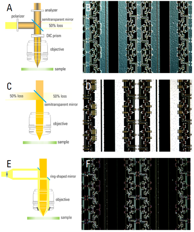
Figure 1. Patterned wafer sample imaged with DIC, brightfield, and darkfield illumination: A) the incident light path in the microscope optics for DIC and B) sample image; C) incident light path for brightfield and D) sample image; and E) incident light path for darkfield and F) sample image. Image Credit: Leica Microsystems GmbH
Challenges When Using DIC
Though DIC enables users to visualize small height differences between structures on a wafer, it can be complex to use for many people. It is essential that the DIC prism is properly adjusted to achieve optimal contrast and accurate, reproducible results. For example, the vertical orientation of sample structures (into or out of the sample horizontal plane) in a DIC image greatly depends how the prisms shears the light waves.
Therefore, shearing influences any height differences observed between structures, i.e., whether one structure in the image appears higher or lower than another. The shearing is generally indicated as having a positive or negative bias (Figure 2), but there is usually no correlation between the bias and the actual height difference.
With most optical microscopes, the DIC prism must be manually adjusted in addition to the polarizer-analyzer crossing. To ensure comparable and consistent DIC results, users generally require a high level of experience. It often takes users a significant amount of time and effort to obtain images with good DIC contrast, as it requires multiple manual adjustments.
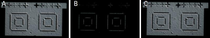
Figure 2. Images of a patterned wafer area taken with DIC having: A) a negative bias, B) no bias, and C) a positive bias. The plus signs and borders of the square shapes appear to rise out of the surface with negative bias and recess into the surface with positive bias. Image Credit: Leica Microsystems GmbH
Advantages of Automated and Reproducible DIC Imaging
During manual DIC operation, the microscope illumination and contrast settings must be adjusted directly by the user. The resulting images are highly reliant on the user’s experience and skill level. However, if using a microscope with automated DIC, wafer inspection workflows can be carried out more efficiently for QC, failure analysis, and R&D.
Users with less experience can perform reproducible DIC imaging easily with minimal changes to settings. With a simple push of a button, the appropriate prism is chosen and its position adjusted for the desired shearing of the incident light wave. In addition, the settings are automatically stored so that they can be easily recalled, which is crucial for reliable documentation when DIC is used.
Leica’s Solution with Reproducible DIC
Six-inch wafers can be inspected quickly and reliably using a DM6 M microscope (Figure 3). It provides reproducible and automated DIC of wafers and semiconductor components, due to its following features:
- A stage specifically designed for six-inch wafers
- An optimally crossed analyzer and polarizer (known as an ICR cube)
- Recall of exact DIC settings with encoded and motorized prism positioning
- A dedicated DIC prism and ICR cube give homogeneous contrast
- It is easy and quick to use because the correct prism and ICR cube are automatically selected and adjusted by the automated microscope.
In addition, the DM6 M has a smaller footprint than other microscopes typically used for wafer inspection, meaning it also saves space in the work area.
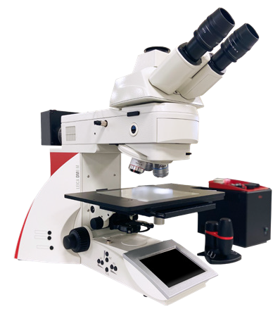
Figure 3. Example of wafer inspection with a DM6 M microscope, which has a 6-inch wafer stage installed. Image Credit: Leica Microsystems GmbH
Figure 4 shows patterned wafer images taken with a DM6 M microscope using reproducible DIC. For comparison, Figure 5 shows images of the same wafer recorded with brightfield and darkfield illumination.
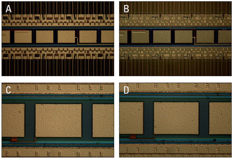
Figure 4. Different areas of a patterned wafer imaged with a DM6 M microscope using DIC with light wave shearing, having a negative (A and C) and positive (B and D) bias. Image Credit: Leica Microsystems GmbH
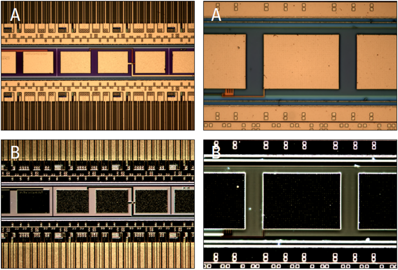
Figure 5. The same areas of the patterned wafer are shown in Figure 4, but now imaged with a DM6 M microscope using A) brightfield and B) darkfield illumination. Image Credit: Leica Microsystems GmbH
Summary and Conclusions
The DM6 M is a six-inch wafer inspection microscope with reproducible and automated differential interference contrast (DIC). Optical microscopy is required for wafer inspection in QC, failure analysis, and R&D in the semiconductor industry. DIC enables efficient visualization of small height differences between structures on patterned wafers. Even users with little experience can efficiently perform DIC imaging during inspection when using an automated and reproducible DIC.
Acknowledgments
Produced using materials originally authored by James DeRose, Raj Saini, and Kay Scheffler from Leica Microsystems.
References
- Diez, D. and DeRose, J. (2020). Metallography – an Introduction. (online) Leica Microsystems. Available at: https://www.leica-microsystems.com/science-lab/industrial/metallography-an-introduction/.
- DeRose, J. and Barbero, D.R. (2023). Rapid Semiconductor Inspection with Microscope Contrast Methods. (online) Leica Microsystems. Available at: https://www.leica-microsystems.com/science-lab/industrial/rapid-semiconductor-inspection-with-microscope-contrast-methods/.

This information has been sourced, reviewed and adapted from materials provided by Leica Microsystems GmbH.
For more information on this source, please visit Leica Microsystems GmbH.