Surfaces are central to materials science. The first few nanometers of a material often determine whether a device performs as intended - or fails.
Examples of surface-driven phenomena include adhesion, catalysis, corrosion resistance, electrochemical activity, and polymer sealing performance.
However, no single analytical instrument can provide all the necessary information. To address this limitation, X-ray Photoelectron Spectroscopy (XPS) and Scanning Electron Microscopy with Energy-Dispersive X-ray Spectroscopy (SEM-EDS) are used together.
This article explains how XPS and SEM-EDS complement each other, highlighting real-world examples, clever techniques, and common pitfalls. These methods construct a more comprehensive and confident understanding of materials.
Two Techniques, Two Perspectives
SEM-EDS: Eyes at the Micron Scale
SEM relies on interactions between electrons and matter. Depending on the selected landing energy, researchers can probe either deep within a material or assess the near-surface region.
- Secondary electrons (SEs): escape only from the very top (a few nanometers), making them ideal for surface detail.
- Backscattered electrons (BSEs): originate deeper and display atomic-number contrast.
- EDS X-rays: come from tens of nanometers to microns deep, unless deliberately running low-kV.
Reducing the SEM beam energy from 10 kV to 1 kV significantly shrinks the electron interaction volume. This increases surface sensitivity and allows the images to complement XPS results. By incorporating energy-filtered detection, SEM becomes capable of near-surface evaluation.
XPS: A Window into Surface Chemistry
XPS operates from the opposite direction: instead of directing electrons at the surface, it uses incident monochromatic X-rays and collects the emitted photoelectrons.
XPS provides:
- Chemical-state information (oxidation, bonding)
- Elemental identification (except H/He)
- Quantitative surface composition
- Sampling depth of only 1-10 nm
Because of its extreme surface sensitivity, XPS excels where SEM-EDS tends to struggle, particularly when chemistry is as important as composition.
Furthermore, with techniques such as angle-resolved XPS (ARXPS) and higher-energy X-ray sources (HAXPES) employing Ag Lα rather than Al Kα, meaningful depth information can be extracted without removing material by ion sputtering.
When XPS and SEM Tell Different Stories and Why That’s a Good Thing
One of the most valuable strategies for materials characterization is to compare SEM-EDS and XPS results from the same area. When the two differ, the discrepancy itself often provides important insight.
The Case of the Hidden GaN Layer
In a model sample containing a GaN structure buried approximately 50 nm beneath the surface:
- XPS observes a laterally homogeneous surface
- SEM-EDS readily detects Ga and N
Rather than indicating failure, this mismatch serves as a depth indicator, revealing the buried layer immediately.
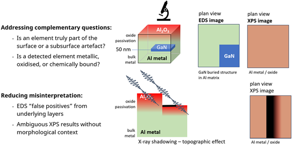
Schematic diagram demonstrating the EDS and XPS images of a passivated aluminum sample with a buried GaN structure. Also, the effect of sample topography causes X-ray shadowing and a resultant XPS image. Image Credit: Kratos Analytical, Ltd.
Considering Topography
Both methods can be tricked by surface characteristics.
- In XPS, steep ridges can shadow the incoming X-ray beam, creating false “elemental voids”
- In SEM-EDS, an off-axis detector can be blocked from seeing X-rays from specific facets
As a result, cross-checking is essential. When XPS and SEM-EDS both reveal structural features in the same area, it is likely a genuine chemical distribution. When only one technique reveals a feature, this may be due to geometric factors rather than chemical ones.
Real-World Examples That Highlight Complementarity
Flexible Packaging: The Opened Seal of a Potato Chip (Crisp) Packet
A multilayer polymer/aluminum laminate was evaluated following a seal opening. Here’s what happened:
- XPS revealed that the aluminum barrier layer was not uniform, with “islands” of exposed Al surrounded by polymer.
- High-resolution XPS measured the Al / Al2O3 ratio, enabling determination of the oxidation Al-passivation layer thickness of 3.3 nm
- Valence-band ‘fingerprints’ identified HDPE as the polymer layer.
This serves as a great example of XPS doing what SEM-EDS simply cannot: identifying chemical states and distinguishing various polymers on the surface.
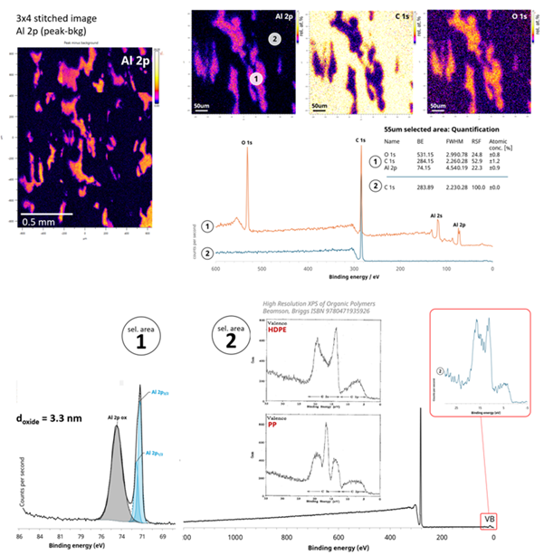
XPS images and selected area spectroscopy from the opened seal of a crisp packet. Non-uniform lateral information reveals the material failure mechanism during the opening of the seal. Image Credit: Kratos Analytical, Ltd.
Graphene on Silicon: An Ideal XPS Application
Graphene, just a few atoms thick, is well-suited for XPS analysis:
- SEM with energy-filtered SE imaging provided useful lateral detail, but could not differentiate the chemical composition
- The C/Si signal ratio provided a practical way to estimate the number of graphene layers
- XPS images exhibited attenuation of the Si 2p signal wherever graphene was present
Here, SEM assists in locating the graphene flake, while XPS helps understand it.
Lithium-Ion Battery Electrodes: Matching Surface and Subsurface Views
On a battery electrode:
- Energy-filtered SEM at 200 V revealed subtle variations in surface potential or composition
- Low-kV EDS (2 kV) detected fluorine distributions that standard high-kV mapping cannot observe
- XPS subsequently confirmed whether those contrasts arose from true chemical differences or simply charging artifacts
This combination, low-kV SEM, low-kV EDS, and XPS, is one of the most effective workflows for battery interfaces.
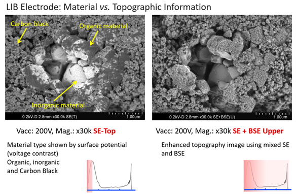
Lithium-ion battery electrode SEM images acquired with a 200 V primary electron beam. On the left, the image is collected using only secondary electrons, whilst the right-hand image is acquired by collecting both secondary and backscattered electrons. Image Credit: Spectral AB
Nanoparticles: Where Both Methods are at Their Limits
Nanoparticles present unique challenges:
- XPS’s sampling depth (a few nanometers) becomes comparable to the particle size
- Nanoparticles agglomerate easily, making interpretation complex.
- SEM-EDS struggles with ultrathin surface coatings without ideal detector geometry
A good example involves core-shell nanoparticles comprising 10 nm Au nanoparticles with approximately one monolayer of Rh:
- Standard EDS detectors did not observe any Rh
- A high-solid-angle annular detector was able to reveal a low-intensity Rh signal
- XPS helped determine the chemical state, while SEM-EDS provided only the presence/absence
This case is a perfect reminder that geometry, sensitivity, and physics play a crucial role at the nanoscale.
A Practical Workflow That Works
A proven sequence that can be used for nearly any advanced material:
1. Begin with SEM (low- to mid-kV)
- Map the terrain
- Identify defects, layers, and inclusions
- Check for topography that might confuse XPS
2. Add SEM-EDS at the lowest feasible kV
- Favor surface-biased X-ray generation
- Use annular/multi-detector setups if available
3. Move to XPS
- Obtain survey + high-resolution core levels
- Utilize angle-resolved or high-energy X-rays for depth insights
- Leverage valence-band spectra for polymers or carbon-rich materials
4. Reconcile the two
- Agreement increases confidence
- Disagreement uncovers hidden structure or geometry
This is where combinatorial data is critical: the two methods complement each other rather than compete.
Conclusion
Although XPS and SEM-EDS operate at different length scales, they can be highly complementary.
SEM-EDS reveals relatively deep structures with exceptional spatial detail, while XPS provides chemical-state information at the uppermost surface. When used together, they provide a more comprehensive and accurate characterization than either alone.
For materials characterization involving thin films, multilayer laminates, and two-dimensional materials such as graphene, catalytic surfaces, or nanoparticles, this combined methodology is essential.
Watch the Accompanying Webinar
Acknowledgements
Produced from materials originally authored by Adam Roberts and Mats Eriksson (Kratos Analytical Ltd & Spectral AB).

This information has been sourced, reviewed, and adapted from materials provided by Kratos Analytical, Ltd.
For more information on this source, please visit Kratos Analytical, Ltd.