Characterizing the motion of microdevices at high frequencies with sub-nanometer resolution is essential for the successful development of next-generation resonant sensor technology.
Microfabrication processes usher in a new era of healthcare technology, with point-of-care sensors promising enhanced sensitivity at low cost and readout times of minutes.
High-quality-factor resonating devices offer the best sensitivity, as adding mass to the sensor shifts the device's resonance frequency. Newcastle University is developing a novel sensing technique based on degenerate vibration modes.
The sensor shape determines the pair of degenerate resonant modes selected. In a perfectly constructed device, symmetry of the system requires that the frequencies of both modes be identical (Figure 1).
Biomolecules can be immobilized to specific regions of the sensor surface, particularly at the antinodal position of one of the modes, breaking this symmetry and splitting the modes' frequencies.
This split is proportional to the mass supplied to the sensor but is insensitive to nonspecific binding events and temperature changes (Figure 2), making it a reliable technology.
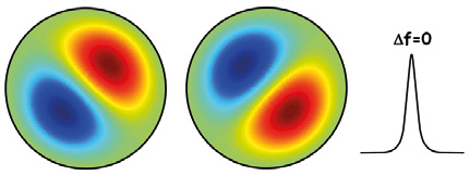
Figure 1. The mode shapes for the (1,0) vibration of a circular diaphragm. For a symmetric device, the modes form a degenerate pair. Image Credit: Polytec
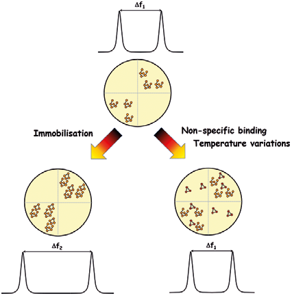
Figure 2. Upon functionalization of the sensor, degeneracy is broken, and the modal frequencies are split by Δf1. Adding mass to the antinodal position of the functionalized mode increases this split to Δf2. For non-specific variations, the split remains unaltered. Image Credit: Polytec
Device Design and Fabrication
Previous sensor designs used a 4.5 µm-thick crystalline silicon diaphragm, which was capacitively operated and detected via electrodes in a sealed compartment beneath the device.
The drawback of this strategy was the use of complex signal recovery circuits, which increased the cost of what would otherwise be a disposable sensor. The most recent design iteration, supported by EPSRC (EP/G061394/1), includes a 750 nm-thick piezoelectric (PZT) layer on the silicon diaphragm.
A 200 nm silicon oxide layer defines electrode regions, and when voltage is applied across an electrode, the generated bending moment pushes the device into motion.
The device is manufactured using cleanroom fabrication procedures. The design must accommodate fabrication tolerances of ±2 µm. A circular diaphragm resonator is formed by bonding two silicon wafers, with one wafer patterned.
A platinum base electrode serves as the foundation layer for the succeeding spun-on PZT thin film, with patterned oxide and gold layers creating the top electrodes and immobilization regions (Figure 3). The wafers are subsequently chopped and packaged as individual devices (Figure 4).
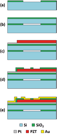
Figure 3. The process flow for the fabrication of the sensor. Image Credit: Polytec
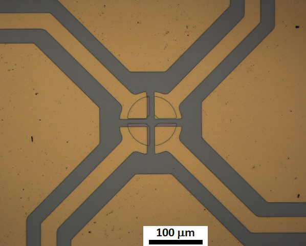
Figure 4. Microscope image of a fabricated sensor. Image Credit: Polytec
Sensor Characterization
Ultimately, device motion is detected using on-board electronics. However, before developing this electronic solution, sensor performance is evaluated using laser Doppler vibrometry. Devices are tested under vacuum, atmospheric pressure, and in a liquid.
Key metrics include resonance frequencies and mode quality parameters. The results show that, due to the PZT's high electromechanical coupling factor, performance between vacuum and atmospheric conditions is comparable. Yet, due to the mass loading in a liquid environment, the performance reduction makes an electronic solution problematic in this scenario.
Mode form alignment is a critical issue in sensitivity. Because the specified geometry determines where molecules will be immobilized on the sensor surface, it is critical that this location matches the antinodal position of the desired mode.
As fabrication errors cause modal misalignment, a precise mapping of each mode form is essential at this stage of development. Electroplating more gold onto the sensor surface assesses mass sensitivity for a given modal alignment.
Results and Future Work
Preliminary results show a device mass sensitivity of 12.0 Hz pg-1 (further information may be found in J. Micromech. Microeng. 23 (2013) 125019). Work is underway to develop frequency-tracking electronics for measuring biomolecule immobilization on the sensor surface.
Preliminary tests of the sensor were conducted with a Polytec fiber-optic vibrometer capable of characterizing frequencies up to 20 MHz. A UHF-120 system, funded by the EPSRC, has expanded the group's characterization capabilities to 1.2 GHz.
This vibrometer update, which scales device sensitivity with operational frequency, enables the investigation of higher-order modes in the current sensor design and the development of ultra-high-frequency surface acoustic wave sensors.
This UHF vibrometer also serves as an external user facility, and Polytec wants to assist other research groups and institutes with the characterization of their high-frequency equipment.

This information has been sourced, reviewed, and adapted from materials provided by Polytec.
For more information on this source, please visit Polytec.