Technology: Optical Measurement Systems
MEMS devices can be optically characterized using several different measurement techniques.
This follows the various available technologies for measuring a wide range of physical parameters (dimension, film thickness, step height, cross-section, roughness, stress, stiction, modulus of elasticity, response time, thermal expansion, resonance frequency, and so on).
Basic optical microscopy, for example, can provide dimensional analysis and deformation measurements through digital image processing.
More advanced optical measurement systems are designed for specialized applications (3D shape measurement, dynamic response, high lateral resolution, and/or high vertical resolution). Table 1 compares generally accessible approaches.
Table 1. Comparison of MEMS optical measurement tools. Source: Polytec
| Technique |
Lateral Resolution (typical) |
Vertical Resolution (typical) |
Static Shape |
Dynamic Response |
Realtime Response |
| AFM (Atomic Force Microscopy) |
0.0001 μm |
0.0001 μm |
3D |
No |
No |
| SEM (Scanning Electron Microscope) |
0.001 μm |
- |
2D |
No* |
No |
| OM (Optical Microscopy) |
<1 μm |
<1 μm |
2D |
No* |
No |
| CM (Confocal Microscopy) |
<1 μm |
<0.01 μm |
3D |
No |
No |
| WLI (White-light Interferometer) |
<1 μm
<0.01 μm ** |
<0.001 μm |
3D |
Yes** |
No |
| DHM (Digital Holographic Microscopy) |
<1 μm
<0.01 μm ** |
<0.001 μm |
3D |
Yes** |
No |
| SVM (Strobe Video Microscopy) |
<1 μm
<0.01 μm ** |
<1 μm |
2D |
Yes** |
No |
| LDV (Laser Doppler Vibrometry) |
<1 μm
<10-6 μm *** |
<10-6 μm *** |
No |
Yes |
Yes |
* Dynamic response possible using video capture techniques
** Dynamic response possible using strobe techniques
*** Resolution for real-time dynamic response – not static
An LDV's ability to take measurements instantaneously, or in real time, makes it approximately six orders of magnitude shorter than any strobe-based technique, with an amplitude resolution approximately six orders of magnitude greater.
Application: Texas Instruments Digital Mirror Device (DMD)
Settling time is an important parameter in micro-mirror applications when the mirror orientation is rapidly changed between tilt states. Speed and accuracy are important performance measures.
Damping coefficients, resonance frequencies, and drive-control signal optimization are complex mirror design aspects that influence settling-time response.
These can be monitored in real time using laser Doppler vibrometry, which offers high sample rates and accuracy. Scan measurements generate 3D visualizations of mirror responses as time-animated sequences.
Measurements are taken using Texas Instruments DMD arrays. The array comprises millions of 12-micron mirrors. Each mirror rotates +/- 12 degrees about a central axis by twisting around a hidden hinge, as shown in Figure 1.
The light projected to an individual pixel is controlled by moving the mirror from the "-" to the "+" state, and the time spent in the "+" state determines the brightness.
The mirrors may flip on and off at a rate of around 50,000 times per second. Further improvements to switching speed would broaden the range of color scales available in the projected image.
Figure 1. Structure of a Texas Instruments micro mirror. Image Credit: Polytec
Figure 2. Time response of an individual point on a mirror. Image Credit: Polytec
Scan measurements are performed on the DMD array using LDV to determine settling-time response and provide a 3D temporal picture of movement.
Figure 2 shows the displacement of a point targeted by the laser measuring spot in the mirror's corner. When rotated 12 degrees to the "+" state, the mirror's corner moves higher and takes a distinctive amount of time to settle into a stable configuration.
During settling, the mirror oscillates at the fundamental torsional resonance with a dampened frequency. By repeating this measurement at coordinate positions across the whole surface, a comprehensive 3D dynamic representation of the mirror movement is obtained for the primary tilt motion, as well as the orthogonal roll and sag motions.
The output is a 3D animation that depicts the exact time sequence for all three axes. Extending the measurement to numerous mirrors in the array enables comparison of the relative phase of motion from mirror to mirror.
These measurements served as a vital gauge of design settling-time performance and will drive future design evolution.
Application: Testing Pressure Sensors on a Wafer-Level
Wafer-level testing can be an effective method of quality control while also reducing the costs associated with packaging MEMS devices that do not meet standards. LDV-based identification of geometrical and material parameters enables real-time measurements that can be quickly automated at the wafer level in a probe station.
The microscope head can be readily mounted on any probe station. Resonance frequency can be measured at a single spot on the structure in milliseconds. The probe station advances to the next device, where the same measurement is repeated.
The process takes about 2 seconds per die, and the result is a wafer map with quantitative Estimated Identification Error, which is used to determine "pass/fail" criteria.
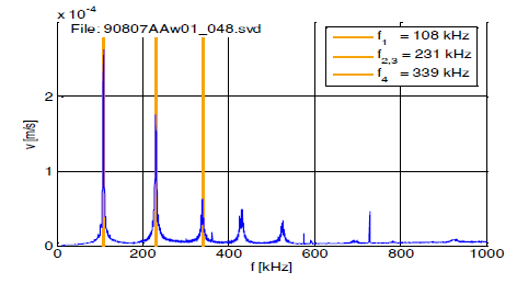
Figure 3A. Frequency response of a good device. Image Credit: Polytec
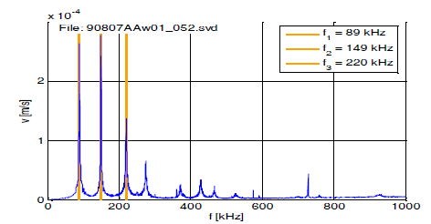
Figure 3B. Frequency response of a bad device. Image Credit: Polytec
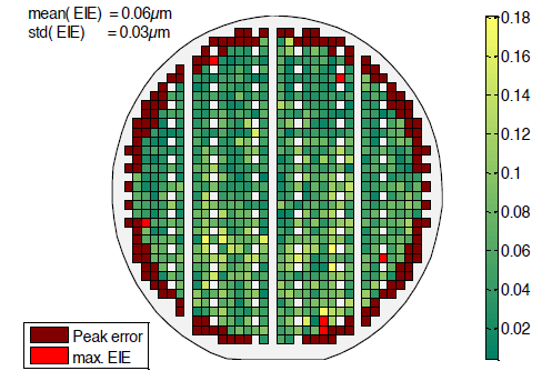
Figure 4. Wafer map of Estimated Identification Error. Bad Devices are shown in red. Image Credit: Polytec
Pressure sensors (1300 µm × 1300 µm) are measured after KOH etching. Parametric testing is based on an algorithm for membrane thickness developed using LDV frequency response measurements.
The membranes are stimulated by contactless electrostatic probes. Figure 3 illustrates the frequency response of two devices.
The first (Figure 3A) shows the frequency response of a "good" die with resonances at predicted frequencies, whereas the second (Figure 3B) depicts a "bad" die with altered resonance frequencies.
The calculation of an Estimated Identification Error (EIE) gives a quantitative evaluation that enables the classification of processing faults. These are mapped on the wafer as illustrated in Figure 4, with a maximum error criterion applied to screen out "bad die" (highlighted in red).
Application: FE Model Validation
In the design phase of MEMS devices, FE models are used to simulate mechanical reactions. Typical models use complicated electrical and mechanical parameters to forecast device response and then design the device to meet goal criteria.
Since many of these values vary owing to fabrication methods, it is critical to validate them through testing. This is especially true during the early stages of manufacture, when the process is less tightly controlled and there are more uncertainties.
A basic example of a MEMS cantilever beam is provided below. The silicon beam measures 225 microns long, 40 microns broad, and 4 microns thick. The resonance frequency (f) is provided by:
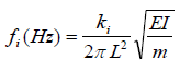
where L is the length, E is the elasticity, I is the moment of inertia, and m is the mass. The modeled geometry is used to create an ANSYS model of the silicon beam with 1,000 nodes.
The initial bending mode is projected to occur at 94,153 Hz (Figure 5, right). Experimental validation of this model is achieved through scanning LDV measurements on the beam, with the same density of measurement points as the model's node points. The experimental findings are compared for validation, and the model is updated using the data.
An idealized model frequently fails to account for complex phenomena such as geometric flaws, non-uniformities, damping, residual stress, mismatched boundary conditions, and torsional compliance.
In this scenario, the experimental results show an initial bending mode at 66,718 Hz (Figure 5, left). The model's use of faulty geometrical values explains this phenomenon.
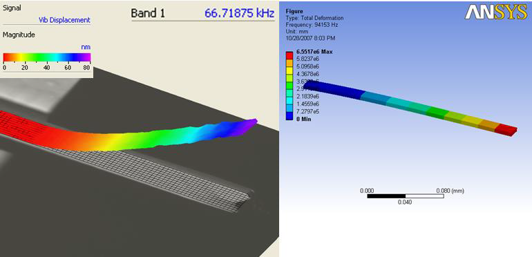
Figure 5. Comparison of cantilever first bending mode determined experimentally (left) and from FE model (right). Image Credit: Polytec
Modeling for inertial sensors can be much more sophisticated in drive-and-sense modes, such as those used in comb drives or tuning fork resonators. These modes are often created for specific frequencies, which must be validated through experimental observations.
Application: Optimizing the Design of Accelerometers
MEMS devices combine electrical and mechanical components to create electromechanical systems.
When characterizing and troubleshooting these devices, it can be difficult to tell whether an observed behavior is entirely mechanical, purely electrical, or inherently both. LDV measurements provide direct mechanical measurements unaffected by electrical effects.
An example measurement is shown for a reliable, robust MEMS low-g servo accelerometer formerly manufactured by Applied MEMS. The accelerometer has a noise floor of around 30 ng/√Hz and a dynamic range of over 115 dB.
The sensor was designed for the harsh conditions of oil exploration, seismic exploration, and monitoring, but it may also be used for inertial navigation, vibration monitoring, and analysis. In the early stages of development, the accelerometer's output shows a spurious resonance about 20 kHz.
Although this frequency is well outside of the acceptable performance band, it is suspected to be the cause of poor sensor performance. The cause of the mode is currently unknown, but there are several possible explanations.
Mechanical sensor modes around this frequency have been identified via FEA simulation, although it is unclear how these modes would manifest in the sensor's closed-loop output. The 20 kHz tone may be caused by control-loop artifacts or package-induced modes.
Figure 6. MEMS accelerometer die from Applied MEMS. Image Credit: Polytec
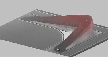
Figure 7. Bending mode of flexure at 23 KHz. Image Credit: Polytec
To better understand the tone’s cause, scanning vibrometry is used to scan the surface of the bare die, as illustrated in Figure 6. Because the device is a variable capacitor with detecting and pushing electrodes on either side of the moving proof mass, one of the electrode caps needed to be removed before scanning the moving parts within.
The decapped die is linked to a high-frequency shaker and mechanically stimulated in the desired band. The entire surface is scanned with broadband input to the shaker, which excites all modes in the band of interest.
This indicated the general location and frequency of the modes on the device being tested. Using this data, higher resolution rapid scans are performed at single frequencies for specific modes at various points on the die. Figure 7 depicts the results of a quick scan across a 1.5 x 1.5 mm segment that includes the accelerometer spring elbow.
The maximum displacement of the spring elbow is 800 nm. The scan clearly showed a mechanical resonance of the spring elbow. Because the LDV test employs only mechanical excitation, electrical causes of the spurious mode can be further avoided.
The scan also reveals other higher-order modes of the spring arm at frequencies close to 1 MHz. As a result, the sensor has been altered to minimize the detrimental effects of this mode. The ensuing sensor designs result in improved device performance and increased yields.
Conclusion
Polytec offers useful measurement tools for the research and development of MEMS devices utilized in real-world applications. Laser Doppler vibrometry allows real-time, wideband measurements of dynamic response with picometer resolution.
The examples in this paper demonstrate how to use this for characterization, troubleshooting, and design optimization of the Texas Instruments DMD array and the applied MEMS accelerometer. In addition, this capacity can be expanded to include quick, automated wafer-level production test measurements.
These measurement techniques provide a unique inside perspective on MEMS devices, shorten design cycles, enhance yield and performance, and ultimately lower product costs.

This information has been sourced, reviewed, and adapted from materials provided by Polytec.
For more information on this source, please visit Polytec.