Manufacturing and failure analysis in the semiconductor industry increasingly depend on imaging methods that reveal internal structure while avoiding sample damage.
Short-wave infrared (SWIR) imaging is now widely regarded as central to semiconductor inspection applications, with SWIR cameras built around InGaAs sensors offering a means of inspecting feature locations that are invisible to a conventional visible-light camera, for example, inside a bonded stack, beneath a silicon surface, or within a finished package.
This article summarizes the application of SWIR imaging across wafer, die, and package inspection. It also outlines the defect types that can be revealed, as well as the primary criteria used to specify a microscope or camera system for a defined application.
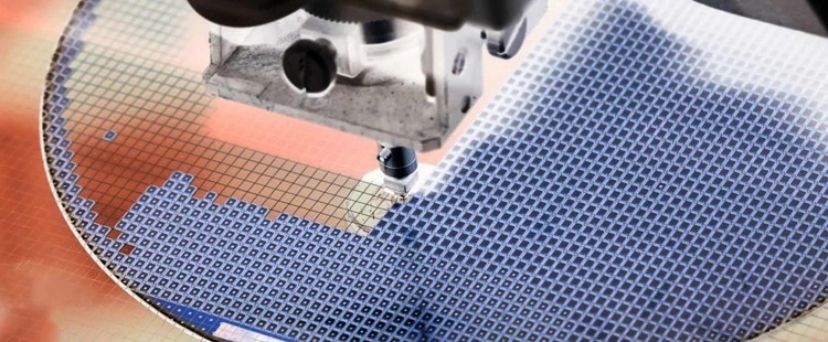
Automated wafer-level inspection: a SWIR-based imaging head scans across a patterned wafer to identify die-level defects prior to dicing. Image Credit: Pembroke Instruments
Limitations of Visible Imaging
Many of the most significant defects in semiconductor processing do not sit at the surface. For example, voids, cracks, misalignment, and contamination are typically found inside a die, at a bonded interface, below the wafer surface, or within an assembled package.
Silicon strongly absorbs visible light, meaning that a standard camera can only report on what is taking place at the outermost surface. It becomes considerably more transmissive at longer, short-wave infrared wavelengths, however.
Silicon’s characteristics mean that an InGaAs SWIR camera operating in the SWIR band can image through the material to reveal internal structures that are unreachable by visible optics.
A sample can be inspected non-destructively in this way, without the polishing, sectioning, or cross-sectioning required by destructive analysis methods.
It is important to note, however, that image quality in this type of setup is not solely determined by the choice of camera.
Parameters such as illumination wavelength, magnification, lens transmission, working distance, sample orientation, field of view, and exposure time all affect the contrast and detail ultimately recoverable from a specific sample.
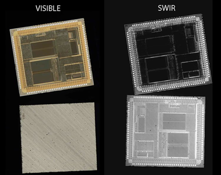
Visible-light imaging (left) shows only the top metallization and packaging surface, while SWIR imaging (right) resolves internal die circuitry through the package and substrate. Image Credit: Pembroke Instruments
SWIR Imaging Applications
It is possible to scale a properly configured SWIR system from a microscope field of view suitable for localized defect review up to a full-wafer, production-line inspection.
Common application areas for SWIR imaging include:
- Silicon wafer inspection, including the identification of edge damage, inclusions, cracks, contamination, and internal non-uniformities that are challenging to determine under visible light.
- Die and IC inspection, including imaging through silicon to locate suspect regions and support non-destructive failure analysis before completing any destructive cross-section work.
- Wafer bonding, including the detection of trapped particles, voids, air gaps, incomplete bonding, and alignment errors between bonded substrates or silicon layers.
- Flip-chip and advanced packaging, including confirming successful alignment and checking internal features in assemblies where visible access is blocked by package materials such as silicon.
- MEMS and TSV analysis, including the examination of internal microstructures, channels, cavities, through-silicon vias, and bonded interfaces, typically with controlled SWIR illumination and microscope optics.
- Solar cell inspection, including the identification of cracks and process-related defects in silicon photovoltaic material via high-resolution SWIR imaging.
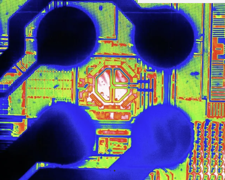
False-color SWIR image of an integrated circuit, with intensity mapped to a color scale to enhance contrast between bond pads, metal routing, and the die's active circuit area. Image Credit: Pembroke Instruments
Detectable Features
Detectability depends on the optical configuration and sample under investigation, but SWIR inspection is generally used to evaluate:
- Wafer cracks, edge damage, and microcracks
- Air gaps, bonding voids, and interface separation
- Wafer, die, or package misalignment
- Embedded particles and contamination
- Internal channels, cavities, vias, and device structures
- Defects hidden under silicon that blocks visible light
- Process non-uniformities and specific material differences
Matching the Camera to the Inspection Task
Sensor resolution is a key specification, but this must be considered against sensitivity, exposure time, field of view, frame rate, available optics, interface type, and illumination. The table below summarizes representative starting points for various inspection needs.
Final camera selection should always be confirmed against current manufacturer specifications and the actual inspection geometry, including a pixel-sampling calculation for the required field of view. Source: Pembroke Instruments
| Inspection Requirement |
Representative Camera Class |
Rationale |
| Highest area-scan detail |
2 MP InGaAs camera, ~1920 × 1080, 8 µm pixels |
Larger field of view combined with finer spatial sampling for detailed wafer or die inspection |
| High resolution, compact footprint |
~1.3 MP InGaAs camera, 1280 × 1024, 10 µm pixels |
Balance of spatial detail, sensitivity, and compact size for flexible integration |
| High-speed / machine vision |
TE-cooled VGA-format InGaAs camera |
Fast acquisition, triggering, and straightforward OEM integration |
Long exposure /
low light |
Low-noise, long-exposure InGaAs camera |
Optimized for applications where available signal is limited |
Micron-scale field
of view |
Configured SWIR microscope system |
Combines camera, objectives, illumination, filters, and stable focus/positioning |
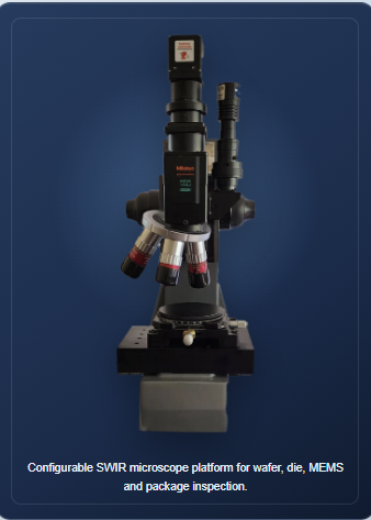
A configurable SWIR microscope platform, adaptable for wafer, die, MEMS, and package-level inspection. Image Credit: Pembroke Instruments
Six Requirements to Define Prior to Specifying a System
1. Smallest Defect to Be Detected
Defining the smallest defect that must be detected will set the required pixel sampling and optical resolution.
2. Field of View
Field of view dictates lens choice and achievable detail, determining whether the target is a full wafer, a die, a package region, or a microscope-scale area.
3. Wavelength and Illumination
Wavelength and illumination must be selected in line with factors such as silicon thickness, transmission versus reflection geometry, sample construction, and required contrast.
4. Inspection Speed
Production-line use defines inspection speed, potentially calling for short exposures, triggering, high frame rates, or region-of-interest readout.
5. Mechanical Geometry
Mechanical geometry incorporates considerations around sample clearance, motion stages, working distance, lens or objective mount, and compatibility with existing equipment.
6. Software and Interface
Interface options include Camera Link, GigE, USB3, or CoaXPress connectivity, along with GenICam, SDK, and triggering, while software environment requirements may include LabVIEW, MATLAB, or custom code.
Summary
SWIR imaging with InGaAs cameras affords failure-analysis teams and semiconductor engineers a means of looking inside a wafer, die, or package without the need for destructive sample preparation.
System design generally involves matching sensor resolution and sensitivity to the required field of view, inspection speed, defect size, and illumination approach, because the achievable result is highly dependent on the overall optical configuration rather than the sensor in isolation. This is typically validated via sample testing prior to specifying a final configuration.
Acknowledgments
Produced from materials originally authored by Pembroke Instruments, LLC.

This information has been sourced, reviewed and adapted from materials provided by Pembroke Instruments, LLC.
For more information on this source, please visit Pembroke Instruments, LLC.