At Fermi National Accelerator Laboratory, materials science brings together fundamental physics and practical engineering in an unusual setting.
Large-scale particle detectors and accelerators are designed, built, and operated by Fermilab. The laboratory’s technology programs also advance capabilities for the next generation, including quantum information science.1
In this environment, the Materials Science Laboratory (MSL) supports superconducting radio-frequency (SRF) resonators in accelerators, and increasingly for superconducting quantum devices.
Zu Hawn Sung, an engineering physicist and member of the Superconducting Quantum Materials and Systems (SQMS) Center’s technology thrust, works at this interface. SQMS is one of five DOE National Quantum Information Science Research Centers. His expertise spans condensed-matter physics and materials science, and he studies quantum devices through the lens of superconductivity.2
Sung has watched the laboratory expand from accelerator superconducting materials toward a quantum mission. The Thermo Scientific Helios DualBeam FIB-SEM has become an important platform for nanoscale characterization and sample preparation in that work.
A Materials Laboratory Built Around Superconductivity
According to Sung, Fermilab organized its Materials Science Laboratory to enable nanoscale characterization of superconducting materials.
A key responsibility involves supporting superconducting radio-frequency (SRF) resonators for particle accelerators, with particular attention to systems based on niobium and related superconducting compounds.
The lab’s work has also grown to include quantum devices. Within SQMS, which is led by Fermilab, Sung now studies quantum devices and applies materials questions first raised by accelerator superconductivity.
That bridge is evident in his publication record, which includes work on hydride precipitates in niobium, from bulk materials for SRF applications to films for superconducting qubits.[3,4]
The real challenge lies in building connections [between] what we find in the microstructure [and] the meaningful physical properties.
Zu Hawn Sung, Engineering Physicist, Fermilab
Why Microstructure Matters to Quantum Performance
For Sung, the value of microscopy is greatest when a high-resolution image leads to an explanation of device physics. A defect may be straightforward to visualize, but determining whether its size, distribution, surrounding strain field, or chemistry measurably changes superconducting performance is the deeper issue.
This relationship is especially difficult to establish for quantum devices. Their microwave performance is typically measured at millikelvin temperatures, far from the conditions of conventional room-temperature SEM characterization.
Hydrogen in niobium illustrates the challenge. Sung notes that hydrogen moves readily through the niobium lattice and can form niobium hydrides as cooling occurs.
At cryogenic temperatures, SQMS researchers recently found evidence of non-superconducting niobium hydride phases in superconducting qubits. Using a bulk 3D niobium resonator as a proxy, they found that more hydrogen sharply lowered the low-field quality factor, and concluded that hydrides likely contribute to quasiparticle losses in qubits.[4]
Such a structure-property relationship explains why correlative characterization matters. Microscopy establishes where defects and phases occur, and complementary measurements reveal whether those features are benign or detrimental to performance.
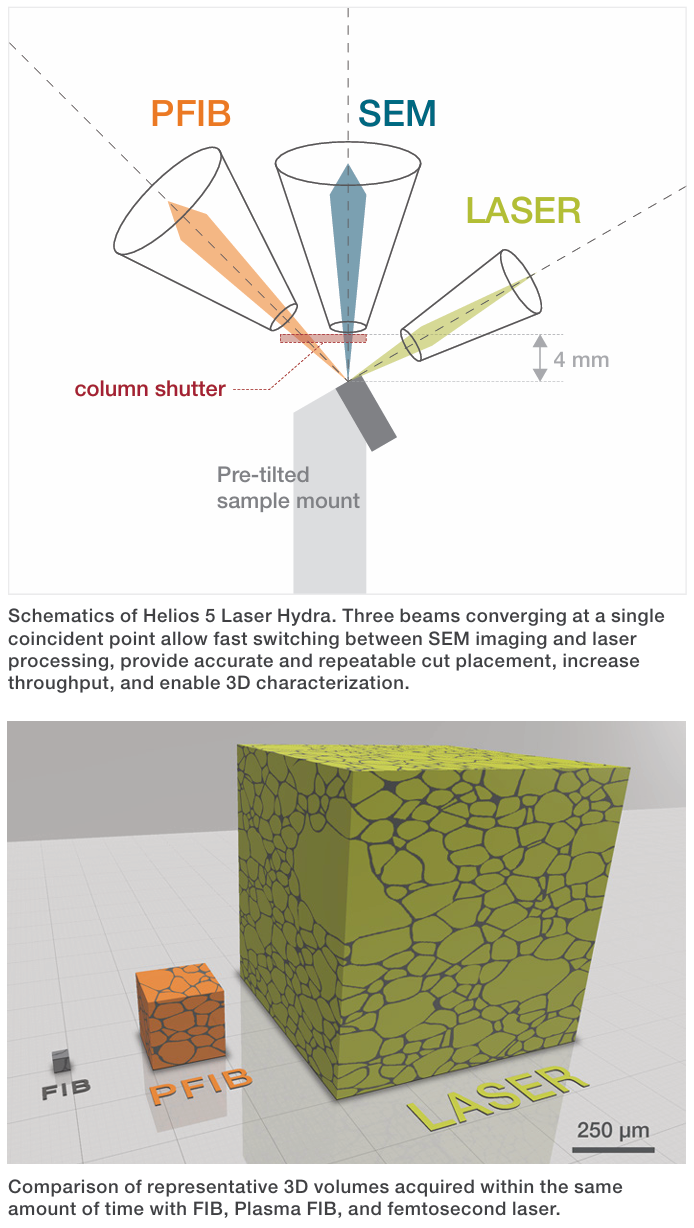
Image Credit: Thermo Fisher Scientific
The Helios DualBeam as a Correlative Materials Platform
Fermilab’s Helios system integrates field-emission SEM imaging and focused ion-beam milling. This combination lets the team move from a surface observation to a site-specific cross-section without losing the region of interest.
Sung describes analyzing crystallography through EBSD and mapping composition through EDS, alongside 3D investigations and cross-sectional analysis of grain structure. Electron-channeling techniques also allow defects and deformation to be observed with the instrument.
Thin lamellae prepared with the system support higher resolution TEM work . It also prepares needle-shaped specimens used in atom probe tomography (APT).
These preparation capabilities place the DualBeam within a larger analytical workflow, where it acts as a gateway rather than an isolated endpoint. Fermilab prepares targeted TEM and APT specimens and collaborates with Northwestern University on high-resolution microscopy and atom probe analysis.
This combination also underlies Thermo Fisher’s positioning of the Helios 5 family: advanced process monitoring, SEM imaging with high resolution, EDS/EBSD integration, and precision in site-specific preparation, including automated or semi-automated workflows.[5]
For a research program in which the scientific question can shift from micrometers to nanometers to atomic chemistry, the benefit is maintaining context as the analysis becomes progressively more localized.
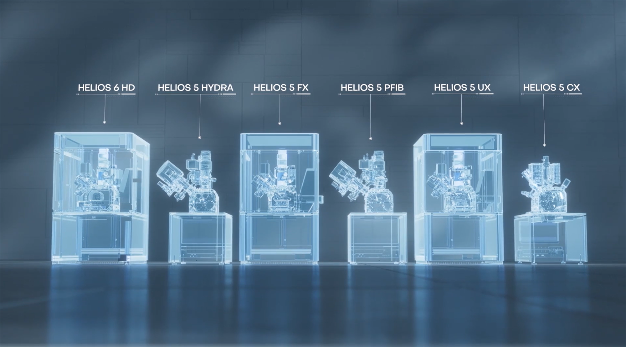
The Thermo Scientific Helios DualBeam Family. Image Credit: Thermo Fisher Scientific
3D Analysis: Seeing the Defect and Its Neighborhood
Three-dimensional characterization is a recurring priority for Sung. Serial sectioning used with EBSD or EDS reveals how grain structure and composition change with depth, providing more than a single polished plane of a complex material.
For superconducting thin films and junction structures, researchers can investigate whether a defect remains isolated or extends through the film, and how the matrix surrounding it changes.
Maximum magnification is only part of his emphasis. As Sung puts it, “million magnification is good for the identified defect,” while the practical objective is often to make the defect and the surrounding microstructure easier to distinguish.
For FIB-SEM development, that distinction is strategically important. For researchers correlating a nanoscale feature with device behavior, nominal resolution may be matched in importance by stable milling and image contrast, precise navigation and endpoint control, and slice-and-view workflows that can be repeated reliably.
Cryogenic Characterization Preserves the Physics
Cryogenic capability matters because some phases that researchers care about, such as niobium hydrides, form only on cooling. Sung investigates hydrides with a cryogenic stage at temperatures around 100K as shown below. At reduced temperature, site-specific cross-sectioning and imaging can help preserve temperature-dependent phases and reduce the risk of changes during warming or handling. As a result, these conditions create a compelling application for cryo-enabled DualBeam workflows
Sung's work may also benefit from the opposite temperature extreme; expanded in situ heating capabilities could enable device-scale studies for SRF applications, potentially approaching 800–900 °C, showing how future microscopy workflows may need to span an increasingly wide range of environmental conditions.
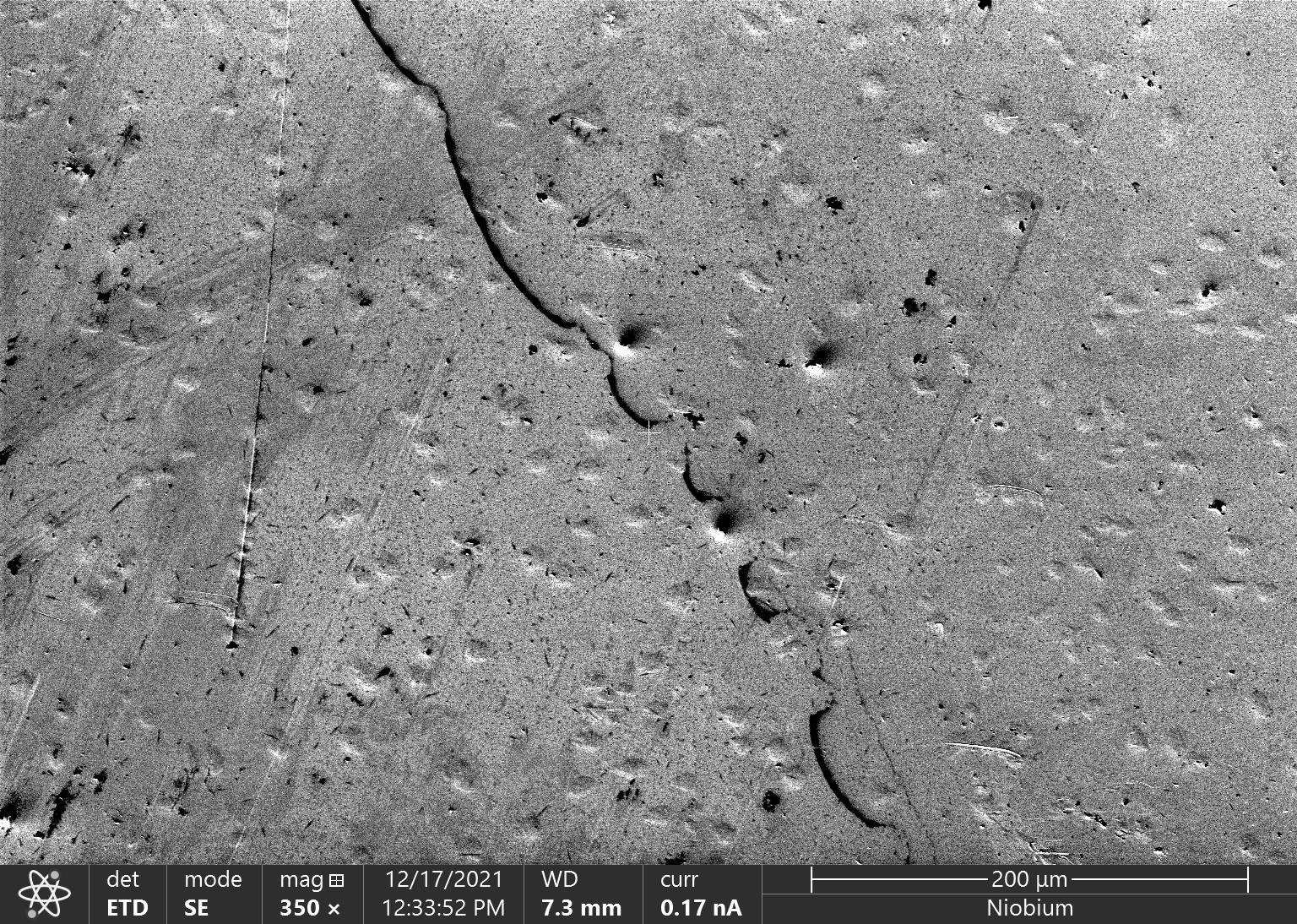
Secondary electron image acquired with LN2 stage of Thermo Scientific Helios DualBeam; niobium hydrides appeared on the surface at 100K. Image Credit: Fermilab
Precision Sample Preparation for TEM and Atom Probe
Sample preparation becomes a science of its own when research questions demand the highest resolution. When lamellae are tens of nanometers thick, the practical challenge is achieving sufficient stability to control the final milling geometry; even small differences in beam profile, positioning, or final polish can be significant.
At this scale, a mature DualBeam workflow can exert a disproportionate influence. Modern Helios 5 configurations are designed to offer low-voltage polishing at the final stage and precision in milling and deposition, as well as automated preparation options and in situ manipulation.5
The importance of these capabilities is evident in Fermilab’s use case. The FIB-SEM must reveal the target and produce a specimen suitable for downstream TEM or APT, without losing the microstructural feature that first motivated the experiment.
A Regional Ecosystem for Quantum Materials
Fermilab’s work is also deeply collaborative. Sung describes frequent contact with regional institutions, including the University of Illinois Chicago, Northwestern University, and the University of Chicago, as well as other institutions in the region. Researchers move between facilities to access complementary instrumentation and expertise.
National laboratories, universities, government institutes, and industry partners come together within SQMS, a multi-institutional center organized around superconducting quantum materials and systems.2
Northwestern offers a particularly illustrative collaboration. Fermilab can locate features and prepare site-specific specimens using its Helios DualBeam, while Northwestern contributes advanced STEM and atom-probe capabilities.
This distributed approach makes instrument compatibility and reproducible preparation strategic assets. With proper preparation, a specimen can carry the scientific question between facilities while preserving the location, structure, and chemistry needed for correlation.
From “Hero” Qubits to Reproducible Quantum Hardware
Quantum research can produce individual devices with high performance, but useful platforms need reproducibility across fabrication runs and across many qubits. A 2026 SQMS study led by Fermilab's materials science group examined 22 transmon qubits across seven chips with a variety of characterization tools. Trench depth, sidewall angle, and surface oxide thickness correlated with variations in energy relaxation time (T1) and together accounted for up to a two-fold variation among nominally identically prepared qubits. Interestingly, macroscopic defects such as scratches showed no clear correlation.[6]
As a result, characterization moves closer to process development and quality control. FIB-SEM, EBSD, EDS, TEM, and APT supply the structural and chemical evidence needed to help explain variation in low-temperature electrical or microwave measurements, complementing those measurements, not replacing them..
Advanced DualBeam platforms therefore present a strategic opportunity to shorten the loop between fabrication, characterization, physical-property measurement, and process refinement, with the emphasis extending beyond imaging for its own sake.
Looking Ahead: More Context, More Correlation, More Control
Sung expects progress to depend on tighter links between microstructure and physical properties. For microscopy, that means reliable handoffs to atomic-scale analysis, three-dimensional context, and temperature control, along with stable preparation and clear contrast between features and matrix. These demands apply to workflows as much as to instruments. Fermilab’s Helios DualBeam is one part of that infrastructure.
Instrumentation, expertise, and collaboration combine to turn a cross-section into scientific understanding, in a field where the performance of quantum devices can hinge on microscopic phases and interfaces.
References and Further Reading
- Fermi National Accelerator Laboratory. About Fermilab. https://www.fnal.gov
- SQMS Center. Zuhawn Sung profile. https://sqmscenter.fnal.gov/profile/zu-hawn-sung/.
- Sung, Z. et al. Direct observation of nanometer size hydride precipitations in superconducting niobium. Scientific Reports 14 (2024). https://doi.org/10.1038/s41598-024-77905-6
- Sung, Z.-H., Bafia, D., Cano, A., Murthy, A., Lee, J.-Y., Reagor, M. J., Rubio-Zuazo, J., Grassellino, A., Romanenko, A. Discovery of niobium hydride precipitates in superconducting qubits. Phys. Rev. Materials 10, 016201 (2026). https://doi.org/10.1103/mgnw-kjps
- Thermo Fisher Scientific. Helios 5 DualBeam. https://www.thermofisher.com/us/en/home/electron-microscopy/products/dualbeam-fib-sem-microscopes/helios-5-dualbeam.html.
- Murthy, A. A. et al. Identifying materials-level sources of performance variation in superconducting transmon qubits. Applied Physics Reviews 13, 021416 (2026). https://pubs.aip.org/aip/apr/article/13/2/021416/3393811
- Sung, Z.-H. (2026). Interview with Zuhawn Sung, Fermilab. Interviewed by Thermo Fisher Scientific. Internal transcript.

This information has been sourced, reviewed, and adapted from materials provided by Thermo Fisher Scientific – Electron Microscopy Solutions.
For more information on this source, please visit Thermo Fisher Scientific – Electron Microscopy Solutions.