Sponsored by XradiaApr 22 2013
The looming transistor scaling limits have driven the semiconductor industry to advance packaging in order to stay in line with Moore's Law. TSVs facilitate advanced semiconductor packaging by achieving system integration through stacking of wafer and chip die in the packaging. However, development of low-cost, high-yield production processes and design of unfailing TSV device architectures remain key barriers to market adoption of sophisticated 3D packaging technology. To address these problems, TSV morphology needs to be observed and quantified and processing and/or operation-induced failures need to be characterized.
Shortcomings of Existing Techniques
Existing methods such as physical cross sectioning have adequate 2D resolution to capture images of cross sections of failures. Nevertheless, the common disadvantage of cross sectioning, respective of the cutting technique, is the slight misalignment of the position of the cut face from the true center of the via. These misalignments result in an off-center chord cross section cut, which is not aligned along the true center diameter section, thus causing discrepancies in skewing estimates of defect formation and morphological measurements of size. This issue becomes more significant when via sizes decrease. As sectioning is destructive in nature, it can damage or totally destroy the failure area. Hence, repeated imaging in order to troubleshoot and observe failure evolution is impossible.
Moreover, sectioning is a time-consuming process, thus a small number of TSVs can only be imaged by this technique. Hence, there is a need for a new TSV analysis method that is non-destructive and capable of providing high resolution in 3D analysis and large-volume statistics for reliability conclusions.
Suitable Solution from Xradia
The UltraXRM-L200 from Xradia is a 3D X-ray microscope with a spatial resolution of down to 50 nm. It can fulfill the resolution requirements to capture images of current and next generation TSVs and can capture 3D images of a large number of TSVs simultaneously. It is non-destructive in nature, thus it can perform time lapse (4D) imaging to explore the structural integrity and reliability of the package under different processing conditions. The synchronized observation of the entire volume of each via in a multiple-via array enables the UltraXRM-L200 to avoid time-intensive location of defects, thus enabling the analysis of multiple vias in one single scan in order to optimize data set statistics on die samples. To take images of the structures on the wafer surface, it is necessary to reduce the full wafer thickness in the location to be imaged to 50 µm. The UltraXRM-L200 provides two resolution and field of view (FOV) pairings: 15 µm FOV for 50 nm resolution and 65 µm FOV for150 nm resolution.
In a study, a wafer, cleaved to 10 x 10 mm exterior size followed by polishing of backside to 50 µm, was analyzed using the UltraXRM-L200. The results of the study are illustrated in Figure 1 and 2.
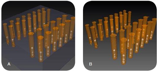
Figure 1. 3D visualization of many vias at once enables location of voids within the copper-filled vias. (A) Shows the vias within the silicon with the voids visible; (B) shows the voids more clearly within the vias. In this scan, rows of 4 µm (top left) and 5 µm (bottom right) vias are sampled simultaneously to compare each process.
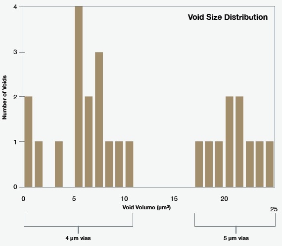
Figure 2. Size distribution of the voids within the metal fills. Two different via diameters were characterized in this scan, generating two separated histograms on this plot.
Conclusion
From the results, it is evident that the UltraXRM-L200 is able to show the discrepancies in void volumes for 4 µm and 5 µm vias by performing localized quantification of defects. The localization of the defect information in each via enables the measurements to provide additional conclusions about failure mechanisms, i.e., plotting the void volume against the via volume in order to correlate the effect of via size to defect growth, or determining processing variability through the measurements of void volume trends along vias in a lateral direction. Non-destructive die-level inspection enables repeated imaging, which can be used to analyze failure evolution in each via as a function of many different variable such as electrical current or heat.

This information has been sourced, reviewed and adapted from materials provided by Xradia.
For more information on this source, please visit Xradia.